Application details, Package outline dimensions – Diodes LMN400B01 User Manual
Page 8
LMN400B01
Document number: DS30699 Rev. 8 - 2
8 of 9
July 2012
© Diodes Incorporated
LMN400B01
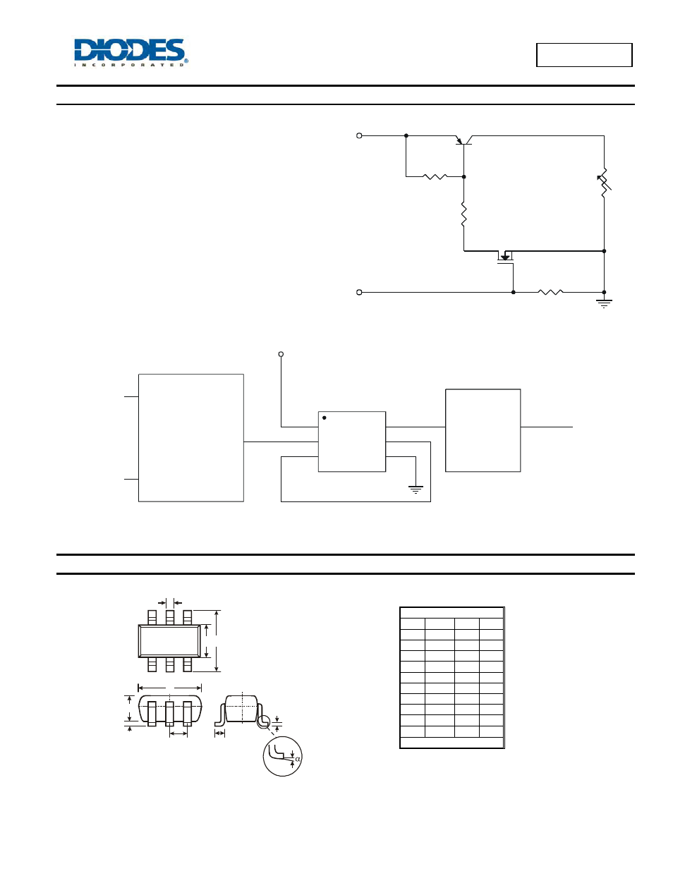
Application Details
PNP Transistor and ESD Protected N-MOSFET integrated as
one in LMN400E01 can be used as a discrete entity for general
applications or as an integrated circuit to function as a Load
Switch. When it is used as the latter as shown in Figure 20,
various input voltage sources can be used as long as it does
not exceed the maximum ratings of the device. These devices
are designed to deliver continuous output load current up to a
maximum of 400mA. The MOSFET Switch draws no current,
hence the loading of the control circuitry is prevented. Care
must be taken for higher levels of dissipation while designing
for higher load conditions. These devices provide high power
and also consume less space. The product mainly helps in
optimizing power usage, thereby conserving battery life in a
controlled load system like portable battery powered
applications. (Please see Figure 21 for one example of a
typical application circuit used in conjunction with a voltage
regulator as a part of power management system).
Vin
Control
D
E
S
B
G
C
Q1
PNP
Q2
NMOSFET
R2
220
R1
10K
37K
LOAD
V
OUT
5V Supply
Vout
Gnd
Vin
Control
U3
Voltage Regulator
IN
OUT
Control Logic
Circuit (PIC,
Comparator
etc)
U1
Vin
OUT1
GND
Diodes Inc.
U2
LMN400B01
1
3
2
4
5
6
E_Q1
D_Q2
G_Q2
S_Q2
B_Q1
C_Q1
Load Switch
Point of
Load
Figure 21 Typical Application Circuirt
Package Outline Dimensions
SOT26
Dim
Min Max Typ
A
0.35 0.50 0.38
B
1.50 1.70 1.60
C
2.70 3.00 2.80
D
⎯
⎯ 0.95
H
2.90 3.10 3.00
J
0.013 0.10 0.05
K
1.00 1.30 1.10
L
0.35 0.55 0.40
M
0.10 0.20 0.15
α
0° 8°
⎯
All Dimensions in mm
Figure 20 Circuit Diagram
A
M
J
L
D
B C
H
K