New prod uc t al8807b, Absolute maximum ratings, Recommended operating conditions – Diodes AL8807B User Manual
Page 3: Electrical characteristics
AL88070B
Document number: DS36191 Rev. 1 - 2
3 of 18
March 2014
© Diodes Incorporated
NEW PROD
UC
T
AL8807B
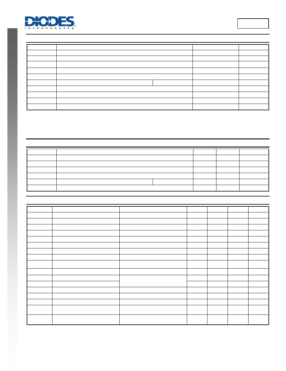
Absolute Maximum Ratings
Symbol
Parameter
Ratings
Unit
ESD HBM
Human Body Model ESD Protection
2.5
kV
ESD MM
Machine Model ESD Protection
200
V
V
IN
Continuous V
IN
Pin Voltage Relative to GND
-0.3 to +40
V
V
SW
SW Voltage Relative to GND
-0.3 to +40
V
V
CTRL
CTRL Pin Input Voltage
-0.3 to +6
V
I
SW-RMS
DC or RMS Switch Current
MSOP-8EP
1.6
A
I
SW-PK
Peak Switch Current (<10%)
2.5
A
T
J
Junction Temperature
+150
°C
T
LEAD
Lead Temperature Soldering
+300
°C
T
ST
Storage Temperature Range
-65 to +150
°C
Caution: Stresses greater than the 'Absolute Maximum Ratings' specified above, may cause permanent damage to the device. These are stress ratings only;
functional operation of the device at these or any other conditions exceeding those indicated in this specification is not implied. Device reliability may be
affected by exposure to absolute maximum rating conditions for extended periods of time.
Semiconductor devices are ESD sensitive and may be damaged by exposure to ESD events. Suitable ESD precautions should be taken when handling
and transporting these devices.
Recommended Operating Conditions
Symbol
Parameter
Min
Max
Unit
V
IN
Operating Input Voltage Relative to GND
6.0
36
V
V
CTRLH
Voltage High for PWM Dimming Relative to GND
2.5
5.5
V
V
CTRLL
Voltage Low for PWM Dimming Relative to GND
0
0.4
V
f
SW
Maximum Switching Frequency
—
1
MHz
I
SW
Continuous Switch Current
MSOP-8EP
—
1.3
A
T
J
Junction Temperature Range
-40
+125
°C
Electrical Characteristics
(V
IN
= 12V, @T
A
= +25°C, unless otherwise specified.)
Symbol
Parameter
Conditions
Min
Typ
Max
Unit
V
INSU
Internal Regulator Start Up Threshold
V
IN
rising
—
—
5.9
V
V
INSH
Internal Regulator Hysteresis Threshold V
IN
falling
100
—
300
mV
I
Q
Quiescent Current
Output not switching (Note 4)
—
—
350
µA
I
S
Input Supply Current
CTRL pin floating f = 250kHz
—
1.8
5
mA
V
TH
Set Current Threshold Voltage
—
95
100
105
mV
V
TH-H
Set Threshold Hysteresis
—
—
±15
—
mV
I
SET
SET Pin Input Current
V
SET
= V
IN
-0.1
—
16
22
µA
R
CTRL
CTRL Pin Input Resistance
Referred to internal reference
—
50
—
kΩ
V
REF
Internal Reference Voltage
—
2.5
—
V
R
DS(ON)
On Resistance of SW MOSFET
I
SW
= 1A
—
0.25
0.4
Ω
t
R
SW Rise Time
V
SENSE
= 100 ±20mV f
SW
= 250kHz
V
SW
= 0.1V~12V~0.1V C
L
= 15pF
—
12
—
ns
t
F
SW Fall Time
—
20
—
ns
T
OTP
Over-Temperature Shutdown
—
—
155
—
°C
T
OTP-Hyst
Over-Temperature Hysteresis
—
—
55
—
°C
I
SW_Leakage
Switch Leakage Current
V
IN
=36V
—
—
0.5
μA
θ
JA
Thermal Resistance Junction-to-
Ambient (Note 5)
(Note 6)
—
69
—
°C/W
θ
JC
Thermal Resistance Junction-to-case
(Note 7)
(Note 6)
—
4.3
—
—
Notes:
4. AL8807B does not have a low power standby mode but current consumption is reduced when output switch is inhibited: V
SENSE
= 0V. Parameter is
tested with V
CTRL
≤ 2.5V.
5. Refer to figure 39 for the device derating curve.
6. Test condition for MSOP-8EP: Device mounted on FR-4 PCB (51mm x 51mm 2oz copper, minimum recommended pad layout on top layer and
thermal vias to bottom layer with maximum area ground plane. For better thermal performance, larger copper pad for heat-sink is needed.
7. Dominant conduction path is via exposed pad.