New prod uc t al8807b, Pin descriptions, Functional block diagram – Diodes AL8807B User Manual
Page 2
AL88070B
Document number: DS36191 Rev. 1 - 2
2 of 18
March 2014
© Diodes Incorporated
NEW PROD
UC
T
AL8807B
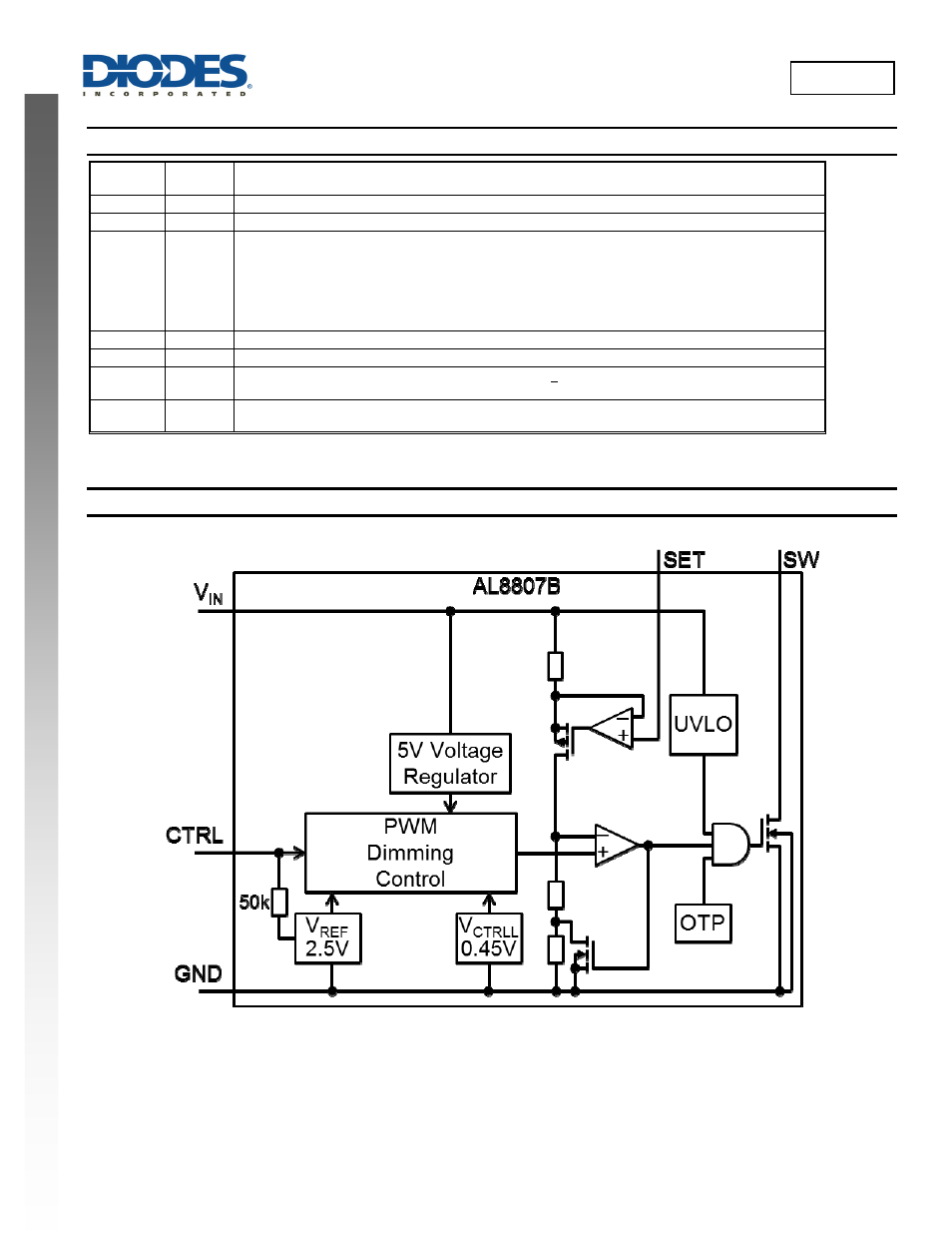
Pin Descriptions
Pin Name
Pin
Number
Function
SET
1
Set Nominal Output Current Pin. Configure the output current of the device.
GND
2, 3
GND Pins
CTRL
4
Dimming and On/Off Control Input.
Leave floating for normal operation.
(V
CTRL
= V
REF
= 2.5V giving nominal average output current I
OUTnom
= 0.1/R
S
)
Drive to voltage below 0.4V to turn off output current
A PWM signal (
2.5V) allows the output current to be adjusted below the level set by the resistor
connected to SET input pin.
SW
5, 6
Switch Pin. Connect inductor/freewheeling diode here, minimizing track length at this pin to reduce EMI.
N/C
7
no connection
V
IN
8
Input Supply Pin. Must be locally decoupled to GND with > 2.2µF X7R ceramic capacitor – see
applications section for more information.
EP
EP
Exposed pad/TAB connects to GND and thermal mass for enhanced thermal impedance. Should not be
used as electrical ground conduction path.
Functional Block Diagram