Applications information, Al9910/a – Diodes AL9910/ AL9910A/ AL9910-5/ AL9910A-5 User Manual
Page 8
AL9910/ AL9910A/ AL9910-5/ AL9910-5A
Document number: DS35103 Rev. 9 - 2
8 of 15
May 2014
© Diodes Incorporated
AL9910/ AL9910A/ AL9910-5/ AL9910A-5
Applications Information
(cont.)
Setting Operating Frequency
The AL9910 is capable of operating over a 25 and 300 kHz switching frequency range. The switching frequency is programmed by connecting an
external resistor between R
OSC
pin and ground. The corresponding oscillator period is:
t
OSC
=
25
22
R
osc
+
µs
with R
OSC
in k
Ω
The switching frequency is the reciprocal of the oscillator period. Typical values for R
OSC
vary from 75k
Ω to 1MΩ
When driving smaller numbers of LEDs, care should be taken to ensure that t
ON
> t
BLANK
. The simplest way to do this is to reduce/limit the
switching frequency by increasing the R
OSC
value. Reducing the switching frequency will also improve the efficiency.
When operating in buck mode the designer must keep in mind that the input voltage must be maintained higher than 2 times the forward voltage
drop across the LEDs. This limitation is related to the output current instability that may develop when the AL9910 operates at a duty cycle greater
than 0.5. This instability reveals itself as an oscillation of the output current at a sub-harmonic
(SBO)
of the switching frequency.
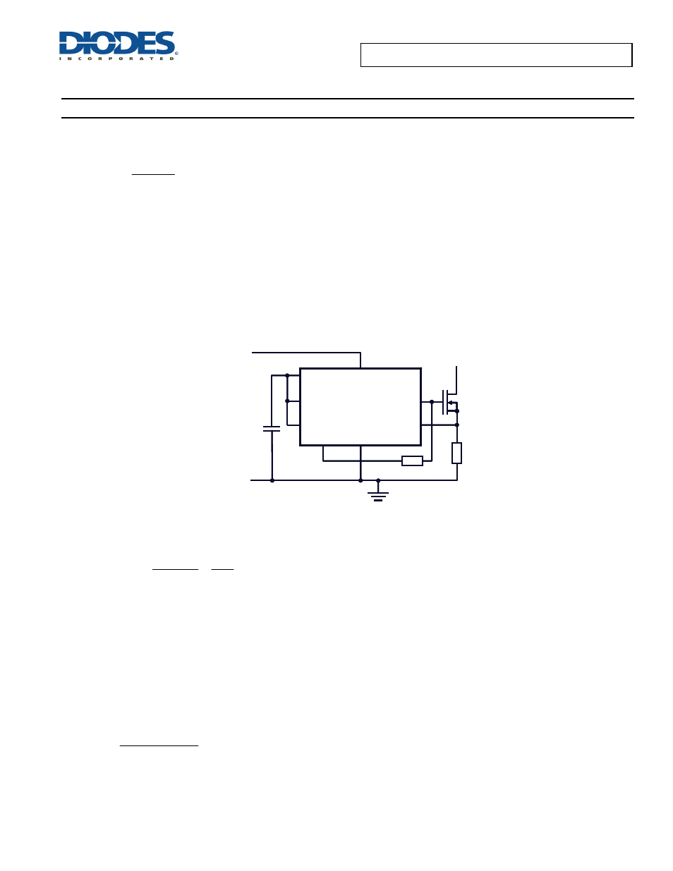
The best solution is to adopt the so-called constant off-time operation as shown in Figure 2. The resistor (R
OSC
) is, connected to ground by
default, to set operating frequency. To force the AL9910 to enter constant OFF time mode R
OSC
is connected to the gate of the external MOSFET.
This will decrease the duty cycle from 50% by increasing the total period, t
OFF
+ t
ON
.
Figure 2. Constant Off-Time Configuration
The oscillator period equation above now defines the AL9910 off time, t
OFF
.
When using this mode the nominal switching frequency is chosen and from the nominal input and output voltages the off-time can be calculated:
OSC
)
nom
(
IN
)
nom
(
OUT
OFF
f
1
V
V
1
t
∗
⎟
⎟
⎠
⎞
⎜
⎜
⎝
⎛
−
=
From this the timing resistor, R
OSC
, can be calculated:
(
)
)
k
(
22
25
)
µs
(
t
R
OFF
OSC
Ω
−
∗
=
Inductor Selection
The non-isolated buck circuit, Figure 1, is usually selected and it has two operation modes: continuous and discontinuous conduction modes. A
buck power stage can be designed to operate in continuous mode for load current above a certain level usually 15% to 30% of full load. Usually,
the input voltage range, the output voltage and load current are defined by the power stage specification. This leaves the inductor value as the
only design parameter to maintain continuous conduction mode. The minimum value of inductor to maintain continuous conduction mode can be
determined by the following example.
The required inductor value is determined from the desired peak-to-peak LED ripple current in the inductor; typically around 30% of the nominal
LED current.
L
=
(
)
(
)
OSC
LED
LEDs
IN
f
I
3
.
0
D
V
V
Ч
Ч
Ч
−
Where D is duty cycle
The next step is determining the total voltage drop across the LED string. For example, when the string consists of 10 High-Brightness LEDs and
each diode has a forward voltage drop of 3.0V at its nominal current; the total LED voltage V
LEDS
is 30V.
AL9910/A
GATE
CS
LD
PWM_D
GND
R
OSC
V
DD
V
IN
Q1
R
OSC
V
IN
AL9910/A
GATE
CS
LD
PWM_D
GND
R
OSC
V
DD
V
IN
Q1
R
OSC
V
IN