Typical applications circuit, Pin descriptions, Functional block diagram – Diodes AL9910/ AL9910A/ AL9910-5/ AL9910A-5 User Manual
Page 2: Al9910/a
AL9910/ AL9910A/ AL9910-5/ AL9910-5A
Document number: DS35103 Rev. 9 - 2
2 of 15
May 2014
© Diodes Incorporated
AL9910/ AL9910A/ AL9910-5/ AL9910A-5
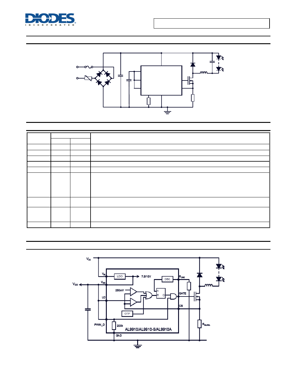
Typical Applications Circuit
Pin Descriptions
Pin
Name
Pin Number
Function
SO-8 SO-8EP
V
IN
1 1
Input Voltage
CS
2
2
Senses LED string and external MOSFET switch current
GND
3 3
Device
Ground
Gate
4
4
Drives the gate of the external MOSFET switch.
PWM_D
5
5
Low Frequency PWM Dimming pin, also Enable input. Internal 200kΩ pull-down to GND.
V
DD
6 6
Internally regulated supply voltage.
7.5V nominal for AL9910 and AL9910-5
10V nominal for AL9910A.
Can supply up to 1 mA for external circuitry. A sufficient storage capacitor is used to provide storage when
the rectified AC input is near the zero crossing.
LD
7 7
Linear Dimming Input. Changes the current limit threshold at current sense comparator and changes the
average LED current.
R
OSC
8 8
Oscillator Control. A resistor connected between this pin and ground sets the PWM frequency. The devices
can be switched into constant off time (PFM) mode by connecting the external oscillator resistor between
R
OSC
pin and the gate of the external MOSFET.
EP PAD
N/A
EP
Exposed Pad (bottom). Connect to GND directly underneath the package.
Functional Block Diagram
R
SENSE
AL9910/A
GATE
CS
LD
PWM_D
GND
R
OSC
V
DD
V
IN
V
AC
IN
Q1
L1
D1
C1
R
OSC
C2
C3
BR1
R
SENSE
AL9910/A
GATE
CS
LD
PWM_D
GND
R
OSC
V
DD
V
IN
V
AC
IN
Q1
L1
D1
C1
R
OSC
C2
C3
BR1