Electrical characteristics – Diodes AL9910/ AL9910A/ AL9910-5/ AL9910A-5 User Manual
Page 4
AL9910/ AL9910A/ AL9910-5/ AL9910-5A
Document number: DS35103 Rev. 9 - 2
4 of 15
May 2014
© Diodes Incorporated
AL9910/ AL9910A/ AL9910-5/ AL9910A-5
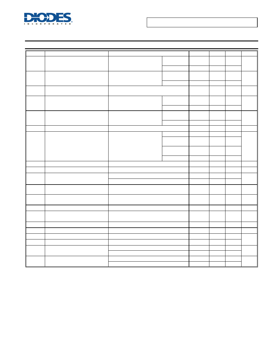
Electrical Characteristics
(@T
A
= +25°C, unless otherwise specified.)
Symbol Parameter
Conditions
Min
Typ
Max
Unit
I
INSD
Shut-Down Mode Supply Current
Pin PWM_D to GND,
V
IN
= V
IN(MIN)
(Note 6)
AL9910
AL9910-5
0.50
1
mA
AL9910A
0.65
1.2
V
DD
Internally Regulated Voltage
V
IN
= V
IN(MIN)
~500V, (Note 8)
l
DD(ext)
= 0, Gate pin open
AL9910
AL9910-5
7.0
7.5
8.0
V
AL9910A
9
10
11
I
DD(ext)
V
DD
Current Available for External
Circuitry
V
IN
= V
IN(MIN)
to 100V (Notes 8 & 9)
1.0
mA
UVLO
V
DD
Under Voltage Lockout Threshold V
DD
rising
AL9910
AL9910-5
6.4
6.7
7
V
AL9910A
8
9
10
∆UVLO V
DD
Under Voltage Lockout Hysteresis V
DD
falling
AL9910
AL9910-5
500
mV
AL9910A
750
R
PWM_D
PWM_D Pull-Down Resistance
V
PWM_D
= 5V
150
200
250
kΩ
V
CS(HI)
Current Sense Threshold Voltage
Full ambient temperature range
(Note 10)
AL9910
225
250
275
mV
AL9910A
230
255
280
AL9910A-5
242
255
267
AL9910-5
237.5
250
262.5
V
GATE(HI)
GATE High Output Voltage
I
OUT
= 10mA
V
DD
-0.3
V
DD
V
V
GATE(LO)
GATE Low Output Voltage
I
OUT
= -10mA
0
0.3
V
f
OSC
Oscillator Frequency
R
OSC
= 1MΩ
20
25
30
kHz
R
OSC
= 226kΩ
80
100
120
D
MAXhf
Maximum Oscillator PWM Duty Cycle
f
PWMhf
= 25kHz, at GATE,
CS to GND.
100
%
V
LD
Linear Dimming Pin Voltage Range
Full ambient temperature range (Note 10),
V
IN
= 20V
0
- 250 mV
t
BLANK
Current Sense Blanking Interval
V
CS
= 0.45V, V
LD
= V
DD
160
250
440
ns
t
DELAY
Delay From CS Trip to GATE lo
V
IN
= 20V, V
LD
= 0.15,
V
CS
= 0 to 0.22V after T
BLANK
300
ns
t
RISE
GATE Output Rise Time
C
GATE
= 500pF
30
50
ns
t
FALL
GATE Output Fall Time
C
GATE
= 500pF
30
50
ns
T
SD
Thermal Shut Down
150
°C
T
SDH
Thermal Shut Down Hysteresis
50
θ
JA
Thermal Resistance Junction-to-
Ambient
SO-8 (Note 11)
110
°C/W
SO-8EP (Note 12)
66
θ
JC
Thermal Resistance Junction-to-Case
SO-8 (Note 11)
22
°C/W
SO-8EP (Note 12)
9
Notes: 8.
V
IN(MIN)
for the AL9910 is 15V and for the AL9910A it is 20V.
9. Also limited by package power dissipation limit, whichever is lower.
10. Full ambient temperature range for AL9910-5S, AL9910AS and AL9910S is -40 to +85°C; for AL9910-5SP, AL9910ASP and AL9910SP is
-40°C to +105°C.
11. Device mounted on FR-4 PCB (25mm x 25mm 1oz copper, minimum recommended pad layout on top. For better thermal performance, larger
copper pad for heat-sink is needed.
12. Device mounted on FR-4 PCB (51mm x 51mm 2oz copper, minimum recommended pad layout on top layer and thermal vias to bottom layer ground
plane. For better thermal performance, larger copper pad for heat-sink is needed.