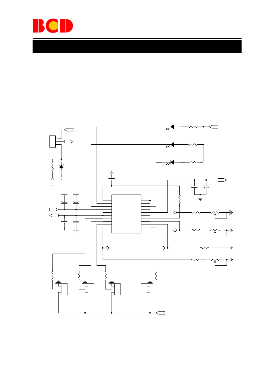
Data sheet, Pc board layout considerations, Figure 13. the evaluation board schematic – Diodes AUR9807 User Manual
Page 20
Data Sheet
Single-cell Li-Ion Charger IC with System Power Management AUR9807
Nov. 2011 Rev. 1. 0 BCD Semiconductor Manufacturing Limited
20
PC Board Layout Considerations
It is important to pay special attention to the PCB
layout. The following provides some guidelines.
1. To obtain optimal performance, the decoupling
capacitor from the input terminal to GND and the
output filter capacitor from OUT to GND should be
placed as close as possible to the AUR9807, with
short trace runs to both signal and GND pins.
2. All low-current GND connections should be kept
separate from the high-current charge or discharge
paths from the battery. Use a single-point ground
technique incorporating both the small signal
ground path and the power ground path.
3. The high-current charge paths into IN and from the
BAT and OUT pins must be sized appropriately for
the maximum charge current in order to avoid
voltage drops in these traces.
V
BAT
R6
100k
R10
10k
JP1
1
2
3
R13
/opt
U1
AUR9807
1
2
3
4
5
6
11
12
9
10
8
7
18
17
16
15
14
13
19
20
VREF
STAT1
STAT2
IN
BAT
BAT
SYSOFF
TS
CE
ISET1
MODE
ISET2
/PG
OUT
OUT
OUT
TMR
APM
GND
GND
LED1 - Green
STAT1
JP5
1
2
3
V
IN
C2
10µF/35V
C1
0.1µF
R16
1k
TP4
TMR
V
OUT
C3
1µF
L
CE
H
R14
30k
C7
/opt
R4
100k
L
MODE
H
H
JP4
1
2
3
L
ISET2
H
JP2
1
2
3
D1
5.1V ZENER
R9
10k
TP1
ISET1
R15
50k
V
OUT
+5V
R5
100k
C6
/opt
V
OUT
V
IN
JP3
1
2
3
R8
1k
R3 1k
R7
100k
R2 1k
R11
27k
C4
10µF/16V
LED3 - Green
/PG
C5
/opt
H
L
SYS_OFF
H
TP3
APM
R1 1k
TP2
TS
H
R12
20k
LED2 - Red
STAT2
Figure 13. The Evaluation Board Schematic