Absolute maximum ratings, Package thermal data, Zxld1374 – Diodes ZXLD1374 User Manual
Page 4: A product line of diodes incorporated
ZXLD1374
Document number: DS35032 Rev. 3 - 2
4 of 39
September 2012
© Diodes Incorporated
ZXLD1374
A Product Line of
Diodes Incorporated
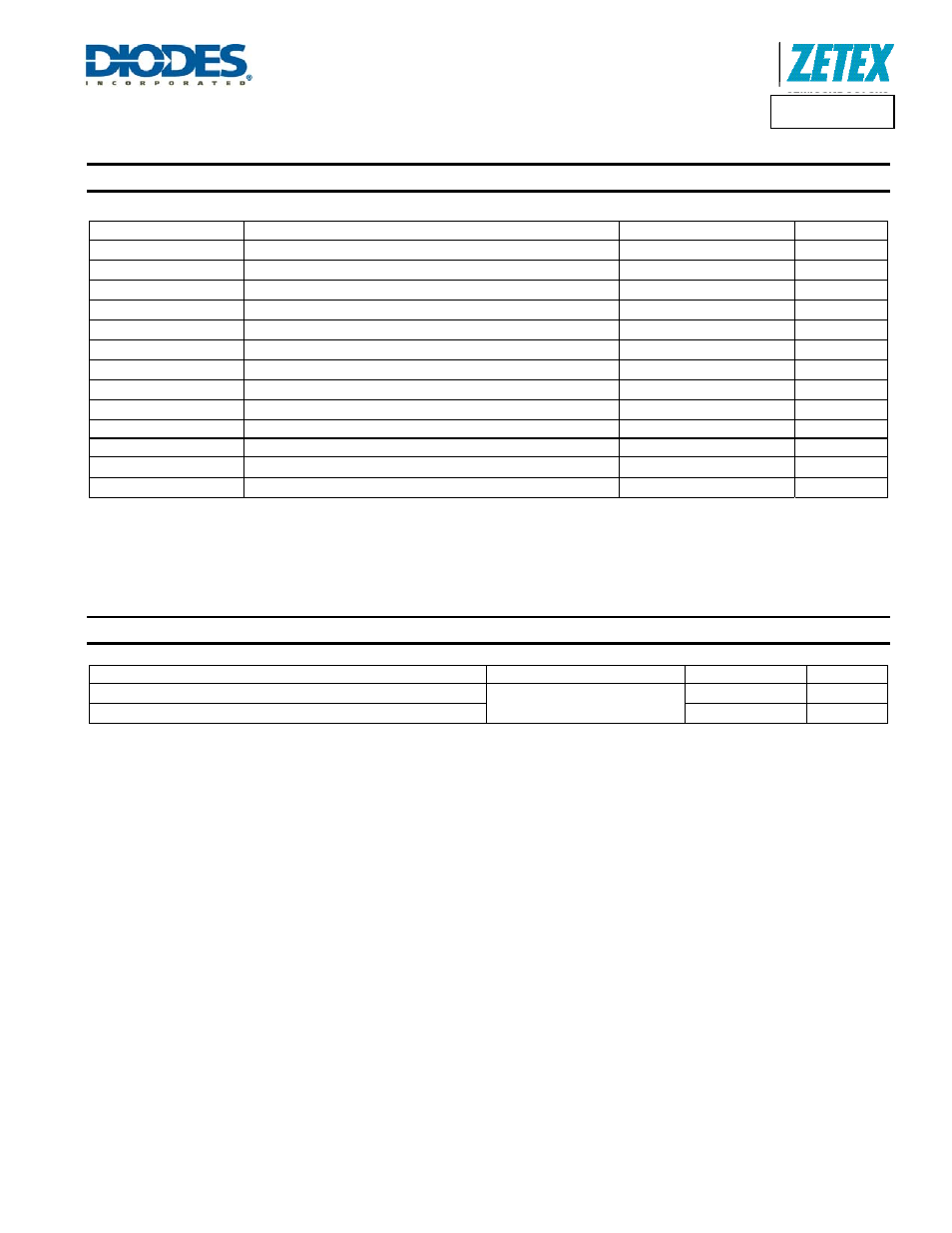
Absolute Maximum Ratings
(Voltages to GND unless otherwise specified.)
Symbol Parameter
Rating
Unit
V
IN
Input Supply Voltage Relative to GND
‡
-0.3 to +65
V
V
AUX
Auxiliary Supply Voltage Relative to GND
‡
-0.3 to +65
V
V
ISM
Current Monitor Input Relative to GND
‡
-0.3 to +65
V
V
SENSE
Current Monitor Sense Voltage (V
IN
-V
ISM
)
-0.3 to +5
V
V
LX
Low Side Switch Output Voltage to GND
‡
-0.3 to +65
V
I
LX
Low Side Switch Continuous Output Current
1.8
A
I
STATUS
Status Pin Output Current
±1
mA
V
FLAG
Flag Output Voltage to GND (Note 5)
-0.3 to +40
V
V
PWM
, V
ADJ
, V
TADJ
, V
GI
Other Input Pins to GND (Note 5)
-0.3 to +5.5
V
ESD HBM
Human Body Model ESD Protection
500
V
ESD CDM
Charged Device Model ESD Protection
1000
V
T
J
Maximum Junction Temperature
150
°C
T
ST
Storage Temperature
-55 to +150
°C
Note: 5.
For
correct operation SGND and PGND should always be connected together.
These are stress ratings only. Operation outside the absolute maximum ratings may cause device failure.
Operation at the absolute maximum rating for extended periods may reduce device reliability.
Semiconductor devices are ESD sensitive and may be damaged by exposure to ESD events. Suitable ESD precautions should be taken when handling and
transporting these devices.
Package Thermal Data
Thermal Resistance
Package
Unit
Junction-to-Ambient, θ
JA
(Note 6)
TSSOP-20EP
28 °C/W
Junction-to-Case, θ
JC
4 °C/W
Note:
6. Measured on High Effective Thermal Conductivity Test Board" according JESD51.