Zxld1374, Application information – Diodes ZXLD1374 User Manual
Page 31

ZXLD1374
Document number: DS35032 Rev. 3 - 2
31 of 39
September 2012
© Diodes Incorporated
ZXLD1374
A Product Line of
Diodes Incorporated
Application Information
(cont.)
PWM Output Current Control & Dimming (cont.)
The PWM pin is designed to be driven by both 3.3V and 5V logic levels. It can be driven also by an open drain/collector transistor. In this case
the designer can either use the internal pull-up network or an external pull-up network in order to speed-up PWM transitions, as shown in the
Boost/ Buck-Boost section.
LED current can be adjusted digitally, by applying a low frequency PWM logic signal to the PWM pin to turn the controller on and off. This will
produce an average output current proportional to the duty cycle of the control signal. During PWM operation, the device remains powered up
and only the output switch is gated by the control signal.
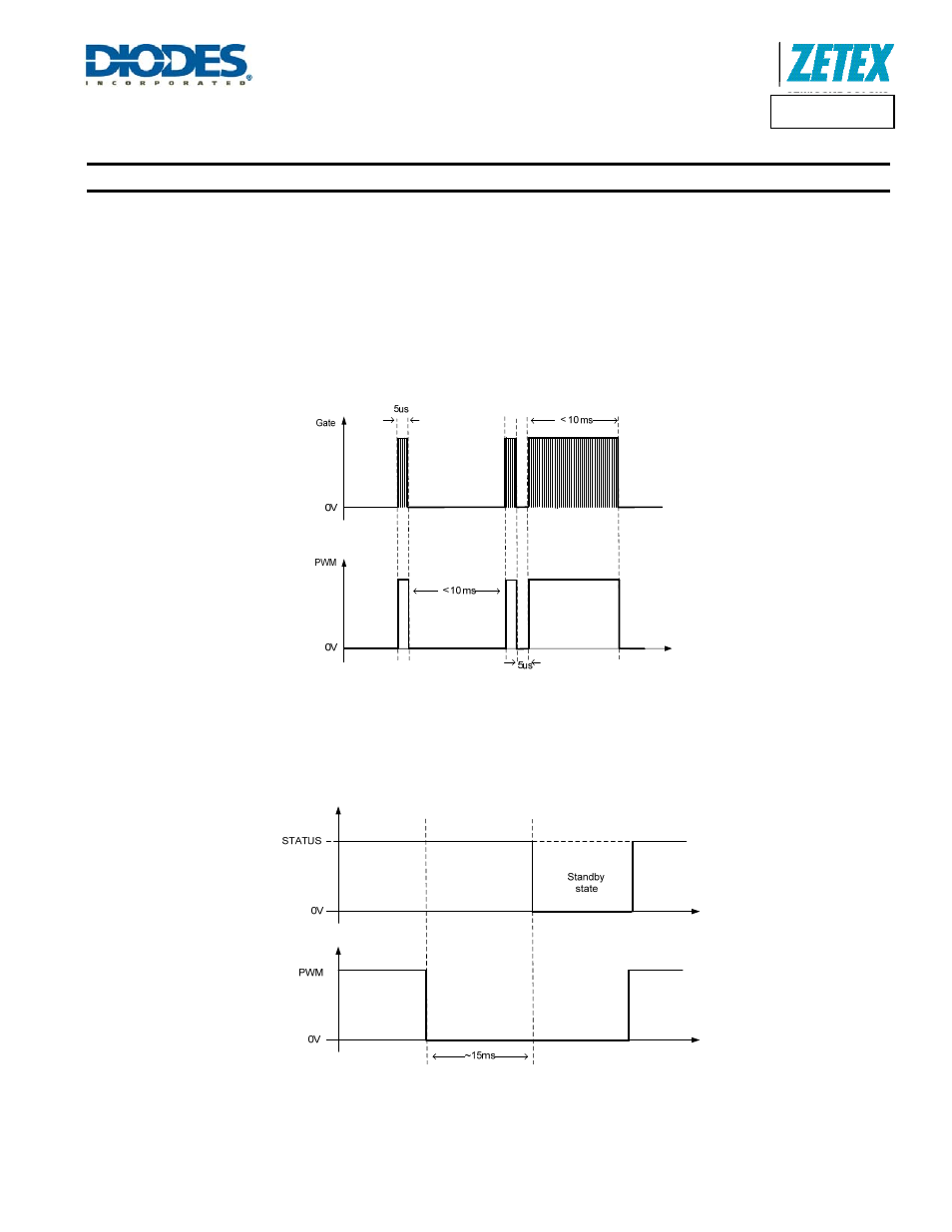
The PWM signal can achieve very high LED current resolution. In fact, dimming down from 100% to 0, a minimum pulse width of 5µs can be
achieved resulting in very high accuracy. While the maximum recommended pulse is for the PWM signal is10ms.
Figure 41 PWM Dimming Minimum and Maximum Pulse
Standby Mode
The device can be put in standby by taking the PWM pin to a voltage below 0.4V for a time exceeding 20ms (15ms nominal). In the shutdown
state, most of the circuitry inside the device is switched off and residual quiescent current will be typically 90µA. In particular, the Status pin will
go down to GND while the FLAG and REF pins will stay at their nominal values.
Figure 42 Stand-By State from PWM Signal
