Zxld1374, Application information – Diodes ZXLD1374 User Manual
Page 33
ZXLD1374
Document number: DS35032 Rev. 3 - 2
33 of 39
September 2012
© Diodes Incorporated
ZXLD1374
A Product Line of
Diodes Incorporated
Application Information
(cont.)
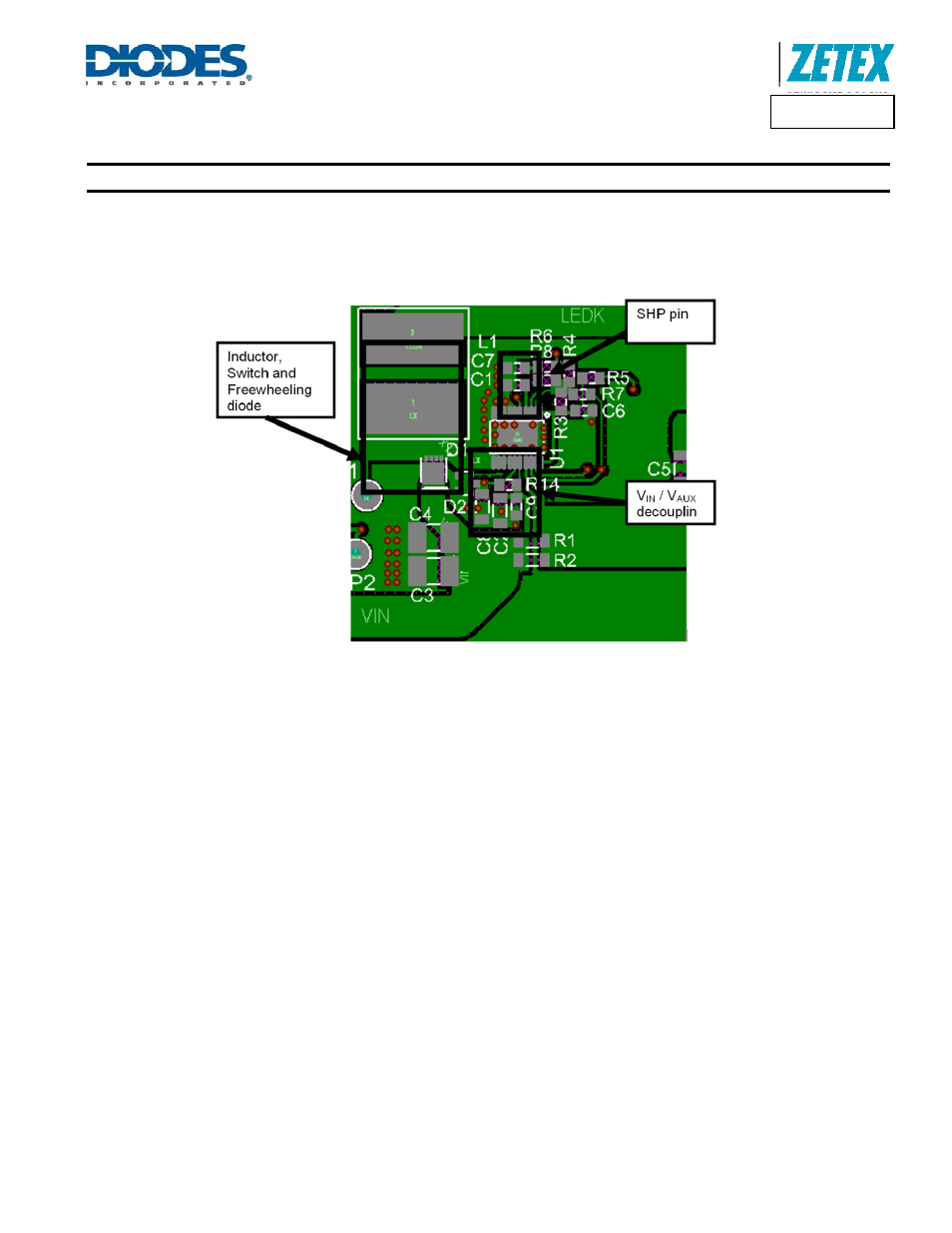
PCB Layout Considerations
PCB layout is a fundamental activity to get the most of the device in all configurations. In the following section it is possible to find some
important insight to design with the ZXLD1374 both in Buck and Buck-Boost/Boost configurations.
Figure 44 Circuit Layout
Here are some considerations useful for the PCB layout:
-
In order to avoid ringing due to stray inductances, the inductor L1, the anode of D1 and the LX pin should be placed as close together as
possible.
-
The shaping capacitor C1 is fundamental for the stability of the control loop. To this end it should be placed no more than 5mm from the
SHP pin.
-
Input voltage pins, V
IN
and V
AUX
, need to be decoupled. It is recommended to use two ceramic capacitors of 2.2µF, X7R, 100V (C3 and
C4). In addition to these capacitors, it is suggested to add two ceramic capacitors of 1µF, X7R, 100V each (C2, C8), as well as a further
decoupling capacitor of 100nF close to the V
IN
/V
AUX
pins (C9) the device is used in Buck mode, or can be driven from a separate
supply.
-
Ensure that there is a large enough thermal mass to keep the thermal impedance between junction and ambient to keep the ZXLD1374
junction temperature below +125°C. On a 2 layer board this means putting enough vias from the landing pad of the TSSOP-20EP
exposed pad through to the bottom layer.