Zxld1374, Application information – Diodes ZXLD1374 User Manual
Page 15

ZXLD1374
Document number: DS35032 Rev. 3 - 2
15 of 39
September 2012
© Diodes Incorporated
ZXLD1374
A Product Line of
Diodes Incorporated
Application Information
The ZXLD1374 is a high accuracy hysteretic inductive Buck/Boost/Buck-boost converter with an internal NMOS switch designed to be used for
current-driving single or multiple series-connected LEDs. The device can be configured to operate in Buck, Boost, or Buck-boost modes by
suitable configuration of the external components as shown in the schematics shown in the device operation description.
Device Operation
a) Buck Mode
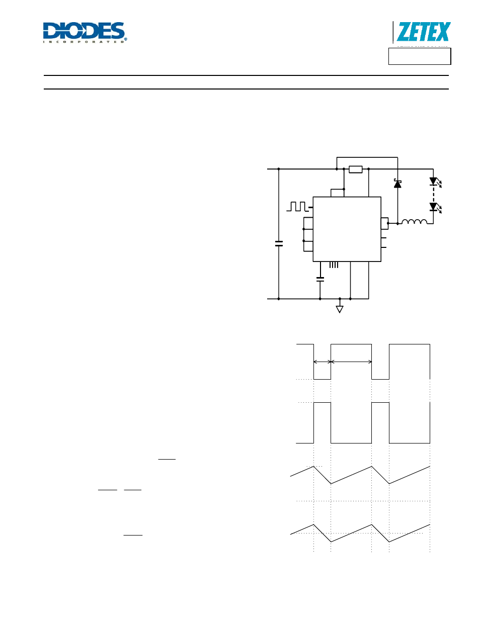
The most simple Buck circuit is shown in Figure 26 LED current
control in Buck mode is achieved by sensing the coil current in the
sense resistor Rs, connected between the two inputs of a current
monitor within the control loop block. An output from the control loop
drives the input of a comparator which drives the gate of the internal
NMOS switch transistor.
When the switch is on, current flows from V
IN
, via Rs, LED, coil and
switch to ground. This current ramps up until an upper threshold
value is reached. At this point the switch is turned off and the current
flows via Rs, LED, coil and D1 back to V
IN
. When the coil current has
ramped down to a lower threshold value the switch is turned on again
and the cycle of events repeats, resulting in continuous oscillation.
The average current in the LED and coil is equal to the average of the
maximum and minimum threshold currents. The ripple current
(hysteresis) is equal to the difference between the thresholds.
The control loop maintains the average LED current at the set level
by adjusting the thresholds continuously to force the average current
in the coil to the value demanded by the voltage on the ADJ pin. This
minimizes variation in output current with changes in operating
conditions.
The control loop also attempts to minimize changes in switching
frequency by varying the level of hysteresis. The hysteresis has a
defined minimum (typ 5%) and a maximum (typ 20%), the frequency
may deviate from nominal in extreme conditions. Loop compensation
is achieved by a single external capacitor C1, connected between
SHP and SGND.
The control loop sets the duty cycle so that the sense voltage is
⎟⎟
⎠
⎞
⎜⎜
⎝
⎛
=
V
V
218
.
0
V
REF
ADJ
SENSE
Therefore,
⎟⎟
⎠
⎞
⎜⎜
⎝
⎛
⎟⎟
⎠
⎞
⎜⎜
⎝
⎛
=
V
V
R
218
.
0
I
REF
ADJ
S
LED
(Buck mode) Equation 1
If the ADJ pin is connected to the REF pin, this simplifies to
⎟⎟
⎠
⎞
⎜⎜
⎝
⎛
=
R
218
.
0
I
S
LED
(Buck mode).
C2
100pF
ZXLD1374
L1
C1
SD1
R1
PWM
VAUXVIN
ISM
GI
ADJ
REF
TADJ
SHP
SGNDPGND
LX
LX
FLAG
STATUS
NC
V
IN
GND
Figure 26 Buck Configuration
GATE
voltage
+11V to
15V typ.
0V
Q1
Drain
voltage
VIN + VF
0V
Coil &
LED
current
0A
I
PK
Sense
voltage
V
IN
- V
ISM
Mean = 218mV
t
OFF
t
ON
Figure 27 Operating Waveforms (Buck Mode)
