Zxld1374, Application information – Diodes ZXLD1374 User Manual
Page 27

ZXLD1374
Document number: DS35032 Rev. 3 - 2
27 of 39
September 2012
© Diodes Incorporated
ZXLD1374
A Product Line of
Diodes Incorporated
Application Information
(cont.)
Reduced Input Voltage Operation
To facilitate operation in applications that have large transient reductions in system supply voltage, the ZXLD1374 is capable of operating down
to input voltages as low as 6.3V. Care must be taken when operating at these lower supply voltages to ensure that the internal MOSFET is
correctly enhanced and that the boosting ratio is not increased to excessive amounts where both the duty cycle and peak-switch current limits
are not exceeded. The device will operate down to 6.3V, but for reliable start up V
IN
must be higher than 6.5V plus any margins for any noise
that may occur on the supply lines.
In Buck-boost and Boost modes (most common topologies for applications likely to require transient operation down to supply voltages
approaching 6V) as the input voltage reduces then the peak switch current will increase the ZXLD1374 compensates for this by allowing the
sense voltage to increase while maintaining regulation of the LED current. However if the boost ratio (switch output voltage/input voltage) is
increased too much then the sense voltage could be increased too much causing an over-current flag to be triggered and/or loss of regulation.
In addition to this, increased power dissipation will occur in the internal MOSFET switch. One way of overcoming this is to apply a boot-strap
network to the V
AUX
pin – see next section.
If the ZXLD1374 is used in buck mode at low voltages then the boot-strap network cannot be implemented and some loss of regulation may
occur at input voltages approaching 6V driving 1 LED.
When using the ZXLD1374 in applications with transient input voltage excursions we recommend using the web calculator to optimize operation
over the normal operating band. Then change the input range to include the transient excursion while keeping the optimized component
selection to check expected function during the transient input voltage conditions.
Boosting V
AUX
Supply Voltage in Boost and Buck-Boost Mode
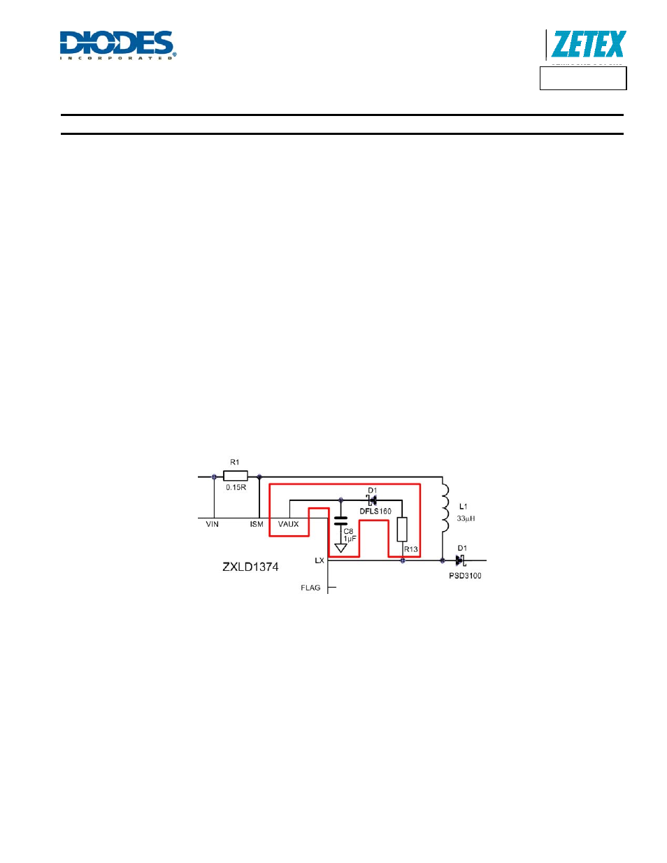
A boot-strap boosting technique can be used to increase the gate drive voltage at low input voltage. See figure 34 for circuit diagram. This can
be particularly important for extended use at low input voltages as this is when the switch current will be at its greatest – resulting in greatest
heat generation within the MOSFET.
Figure 34. Bootstrap Circuit for Boost and Buck-Boost Low Voltage Operations
The Bootstrap circuit guarantees that the MOSFET is fully enhanced reducing both the power dissipation and the risk of thermal runaway of the
MOSFET itself. The bootstrap circuit consists of an extra diode D2 and decoupling capacitor C8 which are used to generate a boosted voltage
at V
AUX
. This enables the device to operate with full output current when V
IN
is at the minimum value of 6.3V. The resistor R13 can be used to
limit the current in the bootstrap circuit in order to reduce the impact of the circuit itself on the LED accuracy. A typical value would be 100 ohms.
The impact on the LED current is usually a decrease of maximum 5% compared to the nominal current value set by the sense resistor.
The Zener diode may be used to limit the voltage on the V
AUX
pin to less than 60V.
Due to the increased number of components and the loss of current accuracy, the bootstrap circuit is recommended only when the system has to
operate continuously in conditions of low input voltage (between 6.3 and 8V) and high load current.
If lower transient voltages are expected then the ZXLD1371 LED Driver-controller could be used, whose input voltage extends down to 5V.
