Zxld1374, Application information – Diodes ZXLD1374 User Manual
Page 16
ZXLD1374
Document number: DS35032 Rev. 3 - 2
16 of 39
September 2012
© Diodes Incorporated
ZXLD1374
A Product Line of
Diodes Incorporated
Application Information
(cont.)
a) Boost and Buck-Boost Modes
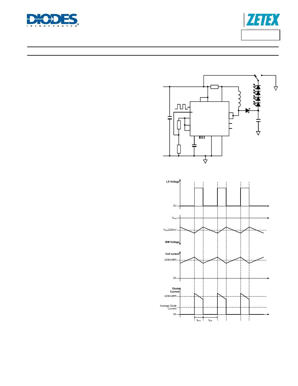
A basic ZXLD1374 application circuit for Buck-Boost and Boost modes is shown in Figure 28.
Control in Boost and Buck-boost mode is achieved by sensing the coil
current in the series resistor Rs, connected between the two inputs of
a current monitor within the control loop block.
An output from the control loop drives the input of a comparator which
drives the gate of the internal NMOS switch transistor. In Boost and
Buck-boost modes, when the switch is on, current flows from V
IN
, via
Rs, coil and switch to ground. The switch current ramps up until an
upper threshold value is reached (see Figure 29). At this point the
switch is turned off and the drain voltage increases to either:
1) the LED chain voltage plus the forward voltage of D1 in Boost
configuration,
or
2) the LED chain voltage plus the forward voltage of D1 plus
VIN in Buck-boost configuration.
The inductor current flows via Rs, coil, D1 and LED back to V
IN
(Buck-boost mode), or GND (Boost mode). When the coil current has
ramped down to a lower threshold value the switch is turned on again
and the cycle of events repeats, resulting in continuous oscillation.
The feedback loop adjusts the NMOS switch duty cycle to stabilize
the LED current in response to changes in external conditions,
including input voltage and load voltage. Loop compensation is
achieved by a single external capacitor C2, connected between SHP
and SGND. Note that in reality, a load capacitor COUT is used, so
that the LED current waveform shown is smoothed.
The average current in the coil is equal to the average of the
maximum and minimum threshold currents and the ripple current
(hysteresis) is equal to the difference between the thresholds. The
average current in the LED, I
LED
, is always less than I
RS
. The
feedback control loop adjusts the switch duty cycle, D, to achieve a
set point at the sense resistor. This controls I
RS
.
During the interval t
OFF
, the coil current flows through D1 and the LED
load.
During t
ON
, the coil current flows through Q1, not the LEDs.
Therefore the set point is modified by D using a gating function to
control ILED indirectly. In order to compensate internally for the effect
of the gating function, a control factor, GI_ADJ is used. GI_ADJ is set
by a pair of external resistors, R
GI1
and R
GI2
. (Figure 28.)
This allows the sense voltage to be adjusted to an optimum level for
power efficiency without significant error in the LED controlled current.
C2
100pF
ZXLD1374
L1
RGI2
RGI2
C1
C
OUT
SD1
R1
PWM
VAUX VIN
ISM
GI
ADJ
REF
TADJ
SHP
SGND PGND
LX
LX
FLAG
STATUS
NC
V
IN
GND
Buck-boost
Boost
Figure 28 Boost and Buck-Boost Configuration
Figure 29 Operating Waveforms
(Boost and Buck-Boost Modes)