Tvs diode arrays, General purpose esd protection - sp1007 series, Diodes) – Littelfuse SP1007 Series User Manual
Page 3: Pulse waveform capacitance vs. reverse bias, Insertion loss (s21) i/o to gnd
© 2013 Littelfuse, Inc.
Specifications are subject to change without notice.
Revised: 11/22/13
TVS Diode Arrays
(SPA
®
Diodes)
General Purpose ESD Protection - SP1007 Series
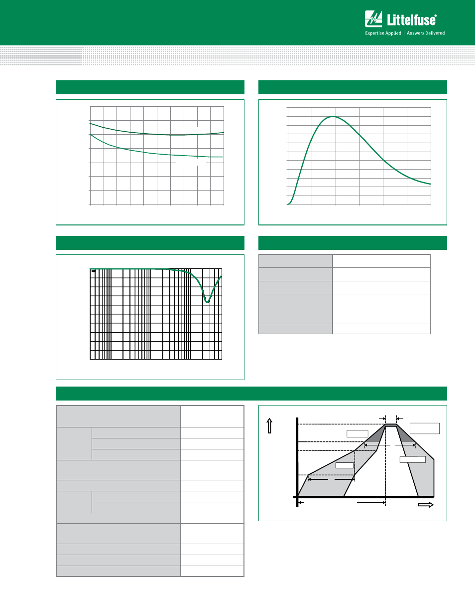
Pulse Waveform
Capacitance vs. Reverse Bias
0.0
0.5
1.0
1.5
2.0
2.5
3.0
3.5
4.0
4.5
5.0
Bias Voltage (V)
Capacitance (pF)
0.0
1.0
2.0
3.0
4.0
5.0
6.0
7.0
SP1007-01ETG
SP1007-01WTG
0%
10%
20%
30%
40%
50%
60%
70%
80%
90%
100%
110%
0.0 5.0 10.0 15.0 20.0 25.0 30.0
Time (μs)
Percent of
I
PP
Insertion Loss (S21) I/O to GND
Frequency (MHz)
At
tenuatio
n
(d
B)
-35
-30
-25
-20
-15
-10
-5
0
-40
-45
10
100
1000
Time
Te
mperatur
e
T
P
T
L
T
S(max)
T
S(min)
25
t
P
t
L
t
S
time to peak temperature
Preheat
Preheat
Ramp-up
Ramp-up
Ramp-down
Ramp-do
Critical Zone
T
L
to T
P
Critical Zone
T
L
to T
P
Reflow Condition
Pb – Free assembly
Pre Heat
- Temperature Min (T
s(min)
)
150°C
- Temperature Max (T
s(max)
)
200°C
- Time (min to max) (t
s
)
60 – 180 secs
Average ramp up rate (Liquidus) Temp
(T
L
) to peak
3°C/second max
T
S(max)
to T
L
- Ramp-up Rate
3°C/second max
Reflow
- Temperature (T
L
) (Liquidus)
217°C
- Temperature (t
L
)
60 – 150 seconds
Peak Temperature (T
P
)
260
+0/-5
°C
Time within 5°C of actual peak
Temperature (t
p
)
20 – 40 seconds
Ramp-down Rate
6°C/second max
Time 25°C to peak Temperature (T
P
)
8 minutes Max.
Do not exceed
260°C
Soldering Parameters
Product Characteristics of SOD-882 Package
Lead Plating
Pre-Plated Frame
Lead Material
Copper Alloy
Lead Coplanarity
0.0004 inches (0.102mm)
Substitute Material
Silicon
Body Material
Molded Epoxy
Flammability
UL 94 V-0
Notes :
1. All dimensions are in millimeters
2. Dimensions include solder plating.
3. Dimensions are exclusive of mold flash & metal burr.
4. Blo is facing up for mold and facing down for trim/form, i.e. reverse trim/form.
5. Package surface matte finish VDI 11-13.