Varistor products, Mhs s eries – Littelfuse MHS Varistor Series User Manual
Page 3
© 2013 Littelfuse, Inc.
25
Revised: December 16, 2013
Varistor Products
MHS S
eries
MHS Varistor Series
Surface Mount Multilayer Varistors (MLVs) > MHS Series
Specifications are subject to change without notice.
Please refer to www.littelfuse.com/series/MHS.html for current information.
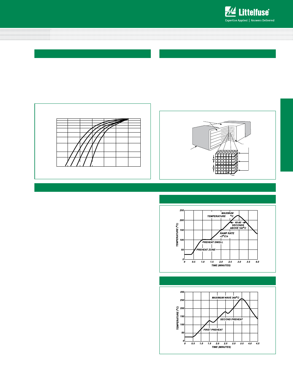
Lead (Pb) Soldering Recommendations
The principal techniques used for the soldering of
components in surface mount technology are IR Re-flow
and Wave soldering. Typical profiles are shown on the right.
The recommended solder for the MHS suppressor is
a 62/36/2 (Sn/Pb/Ag), 60/40 (Sn/Pb) or 63/37 (Sn/Pb).
Littelfuse also recommends an RMA solder flux.
Wave soldering is the most strenuous of the processes.
To avoid the possibility of generating stresses due to
thermal shock, a preheat stage in the soldering process
is recommended, and the peak temperature of the solder
process should be rigidly controlled.
When using a reflow process, care should be taken to
ensure that the MHS chip is not subjected to a thermal
gradient steeper than 4 degrees per second; the ideal
gradient being 2 degrees per second. During the soldering
process, preheating to within 100 degrees of the solder's
peak temperature is essential to minimize thermal shock.
Once the soldering process has been completed, it is
still necessary to ensure that any further thermal shocks
are avoided. One possible cause of thermal shock is hot
printed circuit boards being removed from the solder
process and subjected to cleaning solvents at room
temperature. The boards must be allowed to cool gradually
to less than 50ºC before cleaning.
6.
5.
230
5.0 6.0 7.0
MAXIMUM TEMPERATURE 260˚C
20 - 40 SECONDS WITHIN 5˚C
PREHEAT ZONE
RAMP RATE
<3˚C/s
60 - 150 SEC
> 217˚C
FIGURE 7. LEAD-FREE RE-FLOW PROFILE
6.
5.
230
5.0 6.0 7.0
MAXIMUM TEMPERATURE 260˚C
20 - 40 SECONDS WITHIN 5˚C
PREHEAT ZONE
RAMP RATE
<3˚C/s
60 - 150 SEC
> 217˚C
FIGURE 7. LEAD-FREE RE-FLOW PROFILE
Reflow Solder Profile
Wave Solder Profile
Device Characteristics
At low current levels, the V-I curve of the multilayer
transient voltage suppressor approaches a linear (ohmic)
relationship and shows a temperature dependent effect.
At or below the maximum working voltage, the suppressor
is in a high resistance model (approaching 10
6
Ω at its
maximum rated working voltage). Leakage currents at
maximum rated voltage are below 100µA, typically 25µA;
for 0402 size below 20µA, typically 5µA.
100%
1E
-9
1E
-8
SUPPRESSOR CURRENT (A
DC
)
10%
1E
-7
1E
-6
1E
-5
1E
-4
1E
-3
1E
-2
25
50
75
100
125
o
C
SUPPRESSOR
VO
LT
A
GE IN PERCENT OF
V
NOM
V
ALUE
AT
25
o
C (%)
FIGURE 10. TYPICAL TEMPERATURE DEPENDANCE OF THE CHARACTERISTIC
CURVE IN THE LEAKAGE REGION
o
o
o
o
Typical Temperature Dependance of the Characteristic
Curve in the Leakage Region
Speed of Response
The Multilayer Suppressor is a leadless device. Its response
time is not limited by the parasitic lead inductances found
in other surface mount packages. The response time of the
Z
N
O dielectric material is less than 1ns and the MLE can
clamp very fast dV/dT events such as ESD. Additionally,
in “real world” applications, the associated circuit wiring
is often the greatest factor effecting speed of response.
Therefore, transient suppressor placement within a circuit
can be considered important in certain instances.
GRAINS
DEPLETION
FIRED CERAMIC
DIELECTRIC
REGION
METAL
ELECTRODES
DEPLETION
REGION
METAL END
TERMINATION
FIGURE 11. MULTILAYER INTERNAL CONSTRUCTION
Multilayer Internal Construction
Figure 5
Figure 6
Figure 7
Figure 8