Tvs diode arrays, General purpose esd protection - sp1011 series, Diodes) – Littelfuse SP1011 Series User Manual
Page 2: Absolute maximum ratings, Thermal information, Electrical characteristics, Capacitance vs. reverse bias, Insertion loss (s21) i/o to gnd
© 2013 Littelfuse, Inc.
Specifications are subject to change without notice.
Revised: 10/10/13
TVS Diode Arrays
(SPA
®
Diodes)
General Purpose ESD Protection - SP1011 Series
CAUTION: Stresses above those listed in “Absolute Maximum Ratings” may cause permanent damage to the device. This is a stress only rating and operation of
the device at these or any other conditions above those indicated in the operational sections of this specification is not implied.
Absolute Maximum Ratings
Symbol
Parameter
Value
Units
I
PP
Peak Pulse Current (t
p
=8/20μs)
2
A
T
OP
Operating Temperature
–40 to 125
°C
T
STOR
Storage Temperature
–55 to 150
°C
Thermal Information
Parameter
Rating
Units
Storage Temperature Range
–55 to 150
°C
Maximum Junction Temperature
150
°C
Maximum Lead Temperature (Soldering 20-40s)
260
°C
Electrical Characteristics
(T
OP
=25ºC)
Parameter
Symbol
Test Conditions
Min
Typ
Max
Units
Reverse Voltage Drop
V
R
I
R
= 1mA
6.0
8.5
V
Reverse Standoff Voltage
V
RWM
I
R
≤1µA
6
V
Reverse Leakage Current
I
LEAK
V
R
= 5V
0.1
1
µA
Clamp Voltage
1
V
C
I
PP
=1A, t
p
=8/20μs, Fwd
8.7
V
I
PP
=2A, t
p
=8/20μs, Fwd
10.2
V
Dynamic Resistance
R
DYN
(V
C2
- V
C1
) / (I
PP2
- I
PP1
)
1.5
Ω
ESD Withstand Voltage
1
V
ESD
IEC61000-4-2 (Contact Discharge)
±15
kV
IEC61000-4-2 (Air Discharge)
±30
kV
Diode Capacitance
1
C
D
Reverse Bias = 0V
12
15
pF
Reverse Bias = 2.5V
7
pF
Note:
1. Parameter is guaranteed by design and/or device characterization.
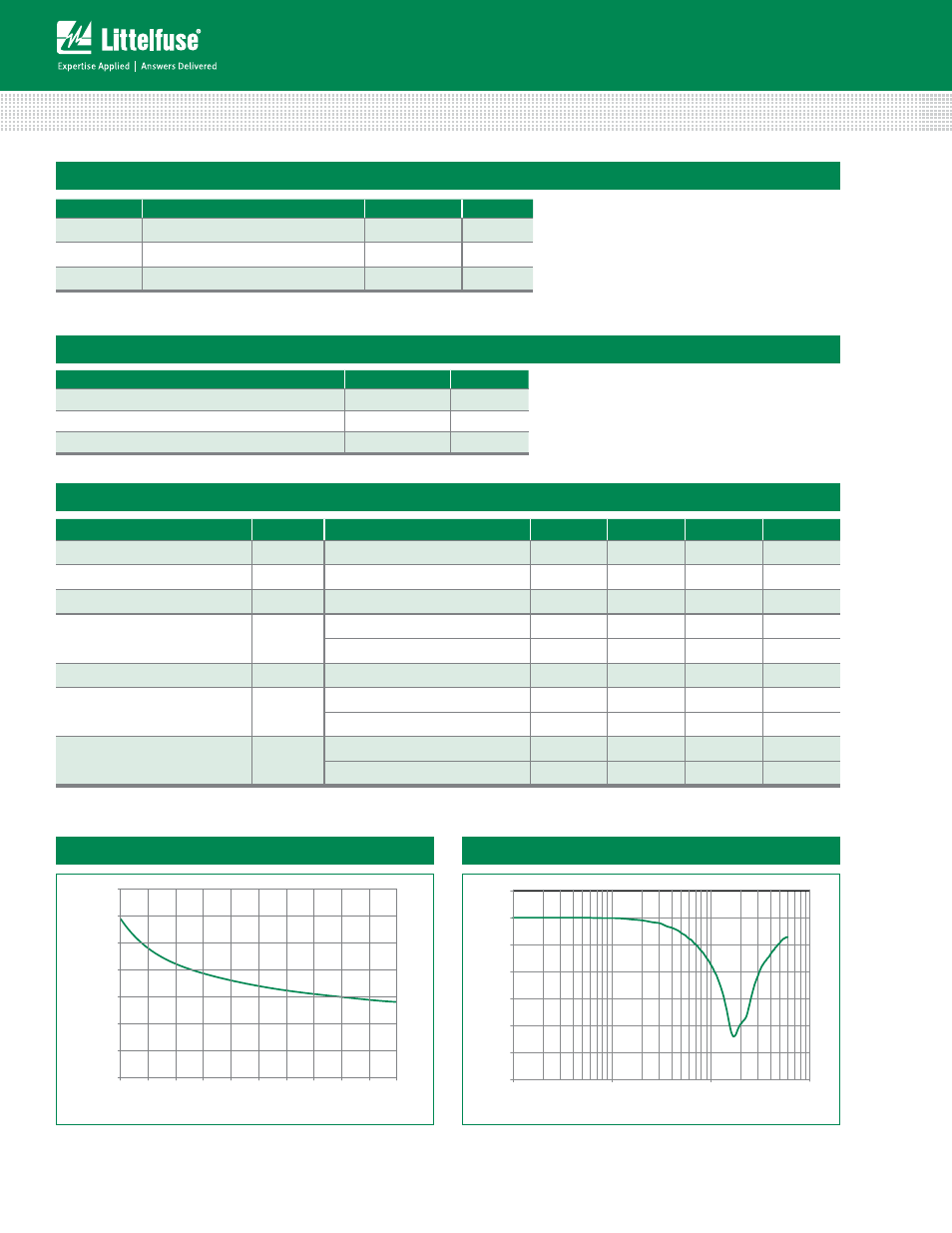
Capacitance vs. Reverse Bias
0.0
2.0
4.0
6.0
8.0
10.0
12.0
14.0
0.0 0.5 1.0 1.5 2.0 2.5 3.0 3.5 4.0 4.5 5.0
DC Bias (V)
Capacitance (pF)
Insertion Loss (S21) I/O to GND
-30
-25
-20
-15
-10
-5
0
5
0
0
0
0
1
0
0
0
1
0
0
1
0
1
Frequency (MHz)
Attenuation (dB)