Tvs diode arrays, General purpose esd protection - sp1006 series, General purpose esd protection – sp1006 series – Littelfuse SP1006 Series User Manual
Page 3: Diodes), Clamping voltage vs. i
© 2013 Littelfuse, Inc.
Specifications are subject to change without notice.
Revised: 04/24/13
TVS Diode Arrays
(SPA
®
Diodes)
General Purpose ESD Protection - SP1006 Series
TVS Diode Arrays
(SPA
®
Diodes)
General Purpose ESD Protection – SP1006 Series
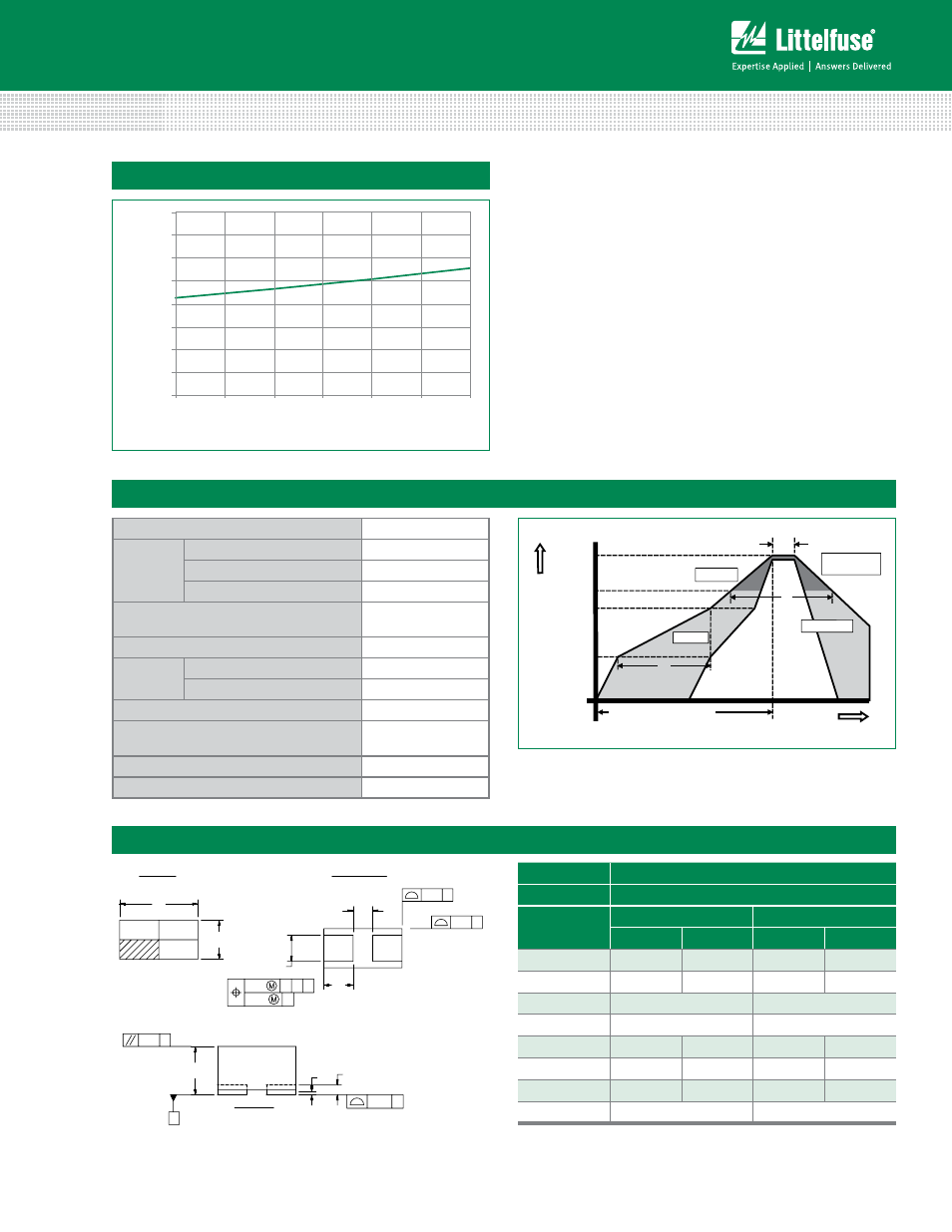
Clamping Voltage vs. I
PP
Peak Pulse Current-I
PP
(A)
Clamp Voltage (V
C
)
0.0
2.0
4.0
6.0
8.0
10.0
12.0
14.0
16.0
1.0
1.5
2.0
2.5
3.0
3.5
4.0
Time
Te
mperatur
e
T
P
T
L
T
S(max)
T
S(min)
25
t
P
t
L
t
S
time to peak temperature
Preheat
Preheat
Ramp-up
Ramp-up
Ramp-down
Ramp-do
Critical Zone
T
L
to T
P
Critical Zone
T
L
to T
P
Reflow Condition
Pb – Free assembly
Pre Heat
- Temperature Min (T
s(min)
)
150°C
- Temperature Max (T
s(max)
)
200°C
- Time (min to max) (t
s
)
60 – 180 secs
Average ramp up rate (Liquidus) Temp (T
L
)
to peak
3°C/second max
T
S(max)
to T
L
- Ramp-up Rate
3°C/second max
Reflow
- Temperature (T
L
) (Liquidus)
217°C
- Temperature (t
L
)
60 – 150 seconds
Peak Temperature (T
P
)
260
+0/-5
°C
Time within 5°C of actual peak
Temperature (t
p
)
20 – 40 seconds
Ramp-down Rate
6°C/second max
Time 25°C to peak Temperature (T
P
)
8 minutes Max.
Soldering Parameters
Package Dimensions — μDFN-2 (0201)
Package
μDFN-2 (0201)
JEDEC
MO-236
Symbol
Millimeters
Inches
Min
Max
Min
Max
A
0.34
0.40
0.014
0.016
A1
0.00
0.05
0.000
0.002
A2
0.075 REF
0.003 REF
b
0.20 REF
0.008 REF
D
0.55
0.65
0.022
0.026
E
0.25
0.35
0.010
0.014
L
0.175
0.275
0.007
0.011
K1
0.15 REF
0.006 REF
D
E
L
2
b
K1
BOTTOM VIEW
TOP VIEW
SIDE VIEW
0.10
0.05
C A B
C
A
C
0.10
A1
A2
0.08
C
SEATING
PLANE
1
2X
2X
0.10
0.10
C
C
General Purpose ESD Protection – SP1006 Series