Rainbow Electronics MAX3799 User Manual
Page 2
MAX3799
1Gbps to 14Gbps, SFP+ Multirate Limiting
Amplifier and VCSEL Driver
2
_______________________________________________________________________________________
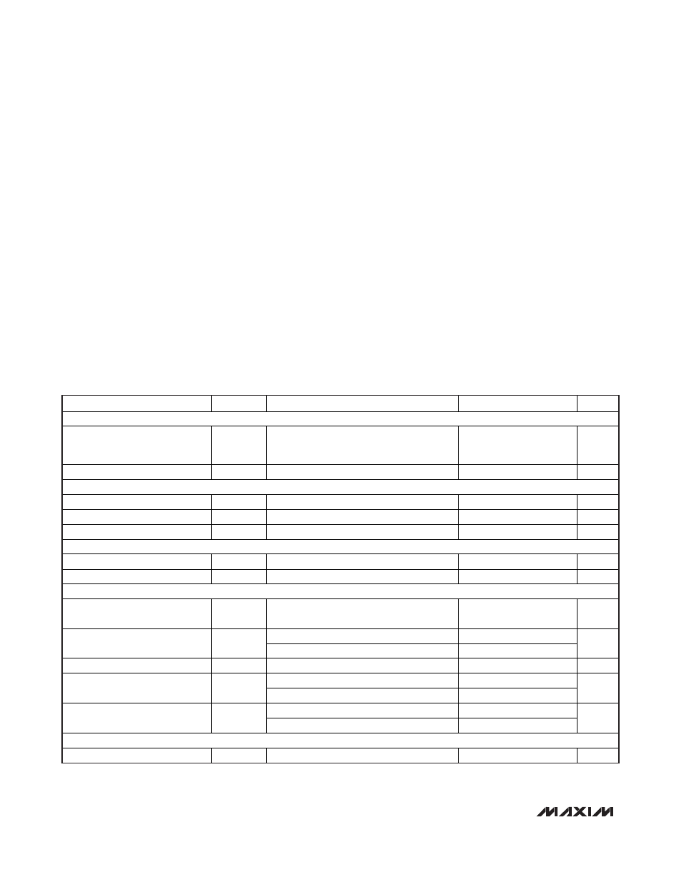
ABSOLUTE MAXIMUM RATINGS
ELECTRICAL CHARACTERISTICS
(V
CC
= 2.85V to 3.63V, T
A
= -40°C to +85°C, CML receiver output load is AC-coupled to differential 100
Ω, C
AZ
= 1nF, transmitter out-
put load is AC-coupled to differential 100
Ω (see Figure 1), typical values are at +25°C, V
CC
= 3.3V, I
BIAS
= 6mA, I
MOD
= 6mA, unless
otherwise specified. Registers are set to default values unless otherwise noted, and the 3-wire interface is static during measure-
ments. For testing, the RATE_SEL bit was used and the RSEL pin was left open.)
Stresses beyond those listed under “Absolute Maximum Ratings” may cause permanent damage to the device. These are stress ratings only, and functional
operation of the device at these or any other conditions beyond those indicated in the operational sections of the specifications is not implied. Exposure to
absolute maximum rating conditions for extended periods may affect device reliability.
V
CCR
, V
CCT
, V
CCD
.................................................-0.3V to +4.0V
Voltage Range at DISABLE, SDA, SCL, CSEL,
RSEL, FAULT, BMON, LOS, CAZ2.........-0.3V to (V
CC
+ 0.3V)
Voltage Range at ROUT+, ROUT- .....(V
CC
- 1V) to (V
CC
+ 0.3V)
Voltage at TIN+, TIN-........................(V
CC
- 2.5V) to (V
CC
- 0.5V)
Voltage Range at TOUT+, TOUT- ......(V
CC
- 2V) to (V
CC
+ 0.3V)
Voltage at BIAS ............................................................0V to V
CC
Voltage at RIN+, RIN- ..........................(V
CC
- 2V) to (V
CC
- 0.2V)
Current Range into FAULT, LOS...........................-1mA to +5mA
Current Range into SDA........................................-1mA to +1mA
Current into ROUT+, ROUT- ...............................................40mA
Current into TOUT+, TOUT- ................................................60mA
Continuous Power Dissipation (T
A
= +70
°C)
32-Pin TQFN (derate 34.5W/°C above +70°C) ...........2759mW
Operating Junction Temperature Range ...........-55°C to +150°C
Storage Temperature Range .............................-65°C to +160°C
PARAMETER SYMBOL
CONDITIONS
MIN
TYP
MAX
UNITS
POWER SUPPLY
Power-Supply Current
I
CC
Includes the CML output current;
excludes I
BIAS
= 6mA, I
MOD
= 6mA,
V
DIFF_ROUT
= 400mV
P-P
(Note 1)
97
150
mA
Power-Supply Voltage
V
CC
2.85 3.63 V
GENERAL
Input Data Rate
1.0625
10.32
Gbps
Input/Output SNR
14.1
BER
10E-12
POWER-ON RESET
High POR Threshold
2.55
2.75
V
Low POR Threshold
I
BIAS
= I
BIASOFF
and I
MOD
= I
MODOFF
2.3
2.45
V
Rx INPUT SPECIFICATIONS
Differential Input Resistance
RIN+/RIN-
R
IN_DIFF
75
100
125
RATE_SEL = 0 (1.25Gbps)
1
3
Input Sensitivity (Note 2)
V
INMIN
RATE_SEL = 1 (10.32Gbps)
3
8
mV
P-P
Input Overload
V
INMAX
1.2
V
P-P
DUT is powered on, f
5GHz
14
Input Return Loss
SDD11
DUT is powered on, f
16GHz
7
dB
DUT is powered on, 1GHz < f
5GHz
8
Input Return Loss
SCC11
DUT is powered on, 1GHz < f
16GHz
8
dB
Rx OUTPUT SPECIFICATIONS
Differential Output Resistance
R
OUTDIFF
75
100
125