Pin description – Rainbow Electronics MAX3799 User Manual
Page 13
MAX3799
1Gbps to 14Gbps, SFP+ Multirate Limiting
Amplifier and VCSEL Driver
______________________________________________________________________________________
13
Pin Description
PIN
NAME
FUNCTION
1 LOS
Loss-of-Signal Output, Open Drain. The default polarity of LOS is high when the level of the input
signal is below the preset threshold set by the SET_LOS DAC. Polarity of the LOS function can be
inverted by setting LOS_POL = 0. The LOS circuitry can be disabled by setting the bit LOS_EN = 0.
2 RSEL
Mode-Select Input, TTL/CMOS. Set the RSEL pin or RATE_SEL bit (set by the 3-wire digital interface)
to logic-high for high-bandwidth mode. Setting RSEL and RATE_SEL logic-low for high-gain mode.
The RSEL pin is internally pulled down by a 75k
resistor to ground.
3, 6, 27, 30
V
CCR
Power Supply. Provides supply voltage to the receiver block.
4
ROUT+
Noninverted Receive Data Output, CML. Back-terminated for 50
load.
5
ROUT-
Inverted Receive Data Output, CML. Back-terminated for 50
load.
7 V
CCD
Power Supply. Provides supply voltage for the digital block.
8 DISABLE
Transmitter Disable Input, TTL/CMOS. Set to logic-low for normal operation. Logic-high or open
disables both the modulation and bias current. Internally pulled up by an 8k
resistor to V
CCT
.
9
SCL
Serial-Clock Input, TTL/CMOS. This pin has a 75k
internal pulldown.
10 SDA
Serial-Data Bidirectional Input, TTL/CMOS. Open-drain output. This pin has a 75k
internal pullup,
but it requires an external 4.7k
pullup resistor to meet the 3-wire digital timing specification. (Data
line collision protection is implemented.)
11 CSEL
Chip-Select Input, TTL/CMOS. Setting CSEL to logic-high starts a cycle. Setting CSEL to logic-low
ends the cycle and resets the control state machine. Internally pulled down by a 75k
resistor to
ground.
12, 15, 18,
21, 24, 25
V
CCT
Power Supply. Provides supply voltage to the transmitter block.
13
TIN+
Noninverted Transmit Data Input, CML
Typical Operating Characteristics—VCSEL Driver (continued)
(V
CC
= 3.3V, T
A
= +25°C, unless otherwise specified. Figure 1 shows the typical setup used for measurements. Registers are set to
default values unless otherwise noted, and the 3-wire interface is static during measurements. For testing, the RATE_SEL bit was
used and the RSEL pin was left open.)
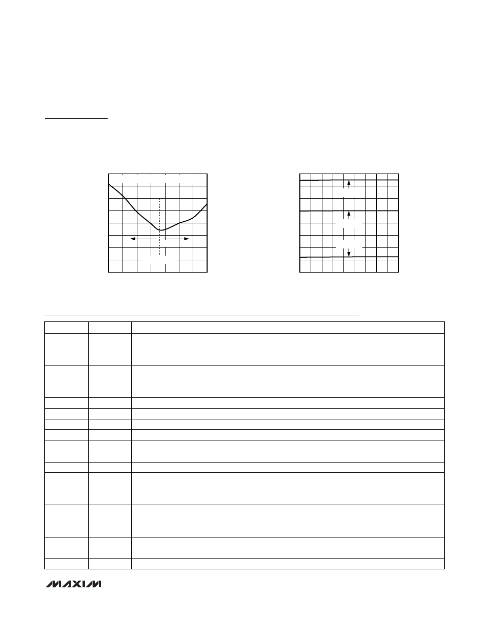
DETERMINISTIC JITTER
vs. PULSE-WIDTH SETTING
MAX3799 toc36
SET_PWCTRL[3:0]
DETERMINISTIC JITTER (ps)
5
3
-5
-3
-1
1
3
4
5
6
7
8
9
10
2
-7
7
PATTERN = PRBS, DATA RATE = 10.32Gbps
EYE CROSSING
DOWN
UP
BIAS MONITOR CURRENT
vs. TEMPERATURE
MAX3799 toc37
TEMPERATURE (
°C)
MONITOR CURRENT (
μ
A)
80
65
-25 -10
5
35
20
50
100
200
300
400
500
600
700
800
0
-40
95
I
BIAS
= 12mA
I
BIAS
= 8mA
I
BIAS
= 2mA