Max109, Typical operating characteristics, Ac electrical characteristics (continued) – Rainbow Electronics MAX109 User Manual
Page 7
MAX109
8-Bit, 2.2Gsps ADC with Track/Hold Amplifier
and 1:4 Demultiplexed LVDS Outputs
_______________________________________________________________________________________
7
AC ELECTRICAL CHARACTERISTICS (continued)
(V
CC
A = V
CC
I = V
CC
D = 5V, V
CC
O = 3.3V, V
EE
= -5V, GNDA = GNDI = GNDD = GNDO = GNDR = 0V, f
CLK
= 2.2Gsps, analog input
amplitude at -1dBFS differential, clock input amplitude 400mV
P-P
differential, digital output pins differential R
L
= 100Ω. Typical values
are at T
A
= +25°C, unless otherwise noted.)
PARAMETER
SYMBOL
CONDITIONS
MIN
TYP
MAX
UNITS
LVDS Output Rise Time
t
RDATA
20% to 80%, C
L
< 2pF
500
ps
LVDS Output Fall Time
t
FDATA
20% to 80%, C
L
< 2pF
500
ps
LVDS Differential Skew
t
SKEW1
Any two LVDS output signals, except DCO
<100
ps
PortD Data Pipeline Delay
t
PDD
7.5
Clock
Cycles
PortC Data Pipeline Delay
t
PDC
8.5
Clock
Cycles
PortB Data Pipeline Delay
t
PDB
9.5
Clock
Cycles
PortA Data Pipeline Delay
t
PDA
10.5
Clock
Cycles
Note 2: Static linearity and offset parameters are computed from a
best-fit straight line through the code transition points. The full-
scale range (FSR) is defined as 255 x slope of the line where the slope of the line is determined by the end-point code tran-
sitions. When the analog input voltage exceeds positive FSR, the output code is 11111111; when the analog input voltage is
beyond the negative FSR, the output code is 00000000.
Note 3: Common-mode rejection ratio is defined as the ratio of the change in the transfer-curve offset voltage to the change in the
common-mode voltage, expressed in dB.
Note 4: The offset-adjust control input is tied to an internal 1.25V reference level through a resistor.
Note 5: Measured with the positive supplies tied to the same potential, V
CC
A = V
CC
D = V
CC
I. V
CC
varies from 4.75V to 5.25V.
Note 6: To achieve 2.8GHz full-power bandwidth, careful board layout techniques are required.
Note 7: The total harmonic distortion (THD) is computed from the second through the 15th harmonics.
Note 8: Guaranteed by design and characterization.
Note 9: RSTOUTP/RSTOUTN are tested for functionality.
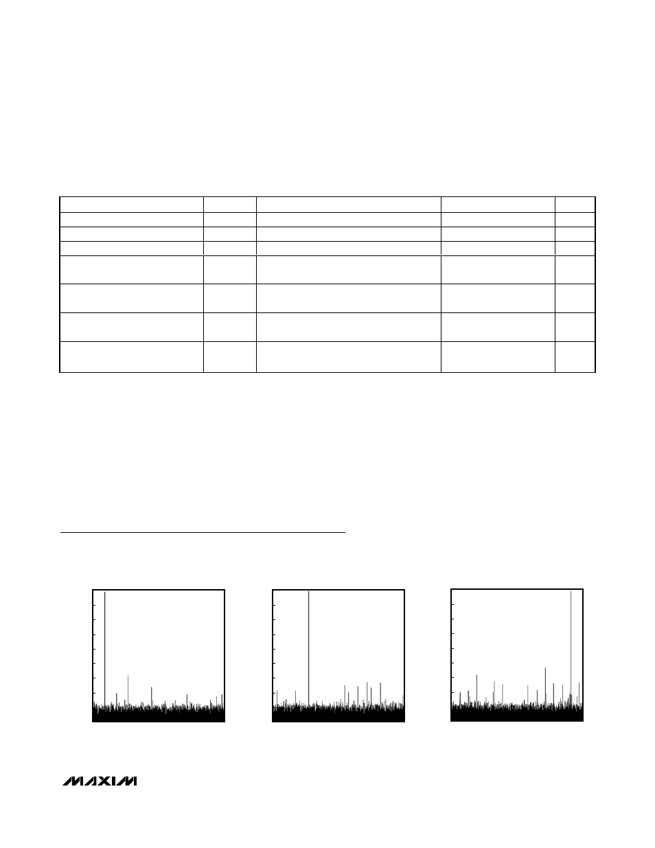
Typical Operating Characteristics
(V
CC
A = V
CC
I = V
CC
D = 5V, V
CC
O = 3.3V, V
EE
= -5V, GNDA = GNDI = GNDD = GNDO = GNDR = 0V, f
CLK
= 2.21184Gsps, analog
input amplitude at -1dBFS differential, clock input amplitude 10dBm differential, digital output pins differential R
L
= 100Ω. Typical
values are at T
J
= +105°C, unless otherwise noted.)
-90
-70
-80
-40
-50
-60
-10
-20
-30
0
FFT PLOT (16,384-POINT DATA RECORD)
MAX109 toc02
AMPLITUDE (dB)
f
CLK
= 2.21184GHz
f
IN
= 300.105MHz
A
IN
= -1.034dBFS
SNR = 45.1dB
SINAD = 44.8dB
THD = -56.2dBc
SFDR = 62.4dBc
HD2 = -64.4dBc
HD3 = -62.7dBc
0
552.96
276.48
829.44
1105.92
414.72
138.24
691.20
967.68
ANALOG INPUT FREQUENCY (MHz)
-90
-70
-80
-40
-50
-60
-10
-20
-30
0
0
552.96
276.48
829.44
1105.92
414.72
138.24
691.20
967.68
FFT PLOT (16,384-POINT DATA RECORD)
MAX109 toc01
ANALOG INPUT FREQUENCY (MHz)
AMPLITUDE (dB)
f
CLK
= 2.21184GHz
f
IN
= 98.145MHz
A
IN
= -0.975dBFS
SNR = 45.2dB
SINAD = 44.8dB
THD = -55.7dBc
SFDR = 57.2dBc
HD2 = -69.6dBc
HD3 = -57.2dBc
-90
-70
-80
-40
-50
-60
-10
-20
-30
0
FFT PLOT (16,384-POINT DATA RECORD)
MAX109 toc03
AMPLITUDE (dB)
f
CLK
= 2.21184GHz
f
IN
= 999.135MHz
A
IN
= -1.059dBFS
SNR = 44.5dB
SINAD = 43.3dB
THD = -49.5dBc
SFDR = 52.1dBc
HD2 = -57.3dBc
HD3 = -52.1dBc
0
552.96
276.48
829.44
1105.92
414.72
138.24
691.20
967.68
ANALOG INPUT FREQUENCY (MHz)