Max109, Bypassing/layout/power supply – Rainbow Electronics MAX109 User Manual
Page 25
integrated fans are available from Co-Fan USA (e.g.,
the 30-1101-02 model, which is used on the evaluation
kit of the MAX109). This particular heatsink with inte-
grated fan is available with pre-applied adhesive for
easy package mounting.
Bypassing/Layout/Power Supply
Grounding and power-supply decoupling strongly influ-
ence the MAX109’s performance. At a 2.2GHz clock
frequency and 8-bit resolution, unwanted digital
crosstalk may couple through the input, reference,
power supply, and ground connections and adversely
influence the dynamic performance of the ADC.
Therefore, closely follow the grounding and power-sup-
ply decoupling guidelines (Figure 17). Maxim strongly
recommends using a multilayer printed circuit board
(PCB) with separate ground and power-supply planes.
Since the MAX109 has separate analog and digital
ground connections (GNDA, GNDI, GNDR, and GNDD,
respectively), the PCB should feature separate analog
and digital ground sections connected at only one
point (star ground at the power supply). Digital signals
should run above the digital ground plane, and analog
signals should run above the analog ground plane.
Keep digital signals far away from the sensitive analog
inputs, reference inputs, and clock inputs. High-speed
signals, including clocks, analog inputs, and digital out-
puts, should be routed on 50Ω microstrip lines, such as
those employed on the MAX109 evaluation kit.
The MAX109 has separate analog and digital power-
supply inputs:
• V
EE
(-5V) is the analog and substrate supply
• V
CC
I (5V) to power the T/H amplifier, clock distribu-
tion, bandgap reference, and reference amplifier
• V
CC
A (5V) to supply the ADC’s comparator array
• V
CC
O (3.3V) to establish power for all LVDS-based
circuit sections
• V
CC
D (5V) to supply all logic circuits of the data con-
verter
The MAX109 V
EE
supply contacts must not be left open
while the part is being powered up. To avoid this condi-
tion, add a high-speed Schottky diode (such as a
Motorola 1N5817) between V
EE
and GNDI. This diode
prevents the device substrate from forward biasing,
which could cause latchup. All supplies should be
decoupled with large tantalum or electrolytic capacitors
at the point they enter the PCB. For best performance,
bypass all power supplies to the appropriate grounds
with a 330µF and 33µF tantalum capacitor to filter power-
supply noise, in parallel with 0.1µF capacitors and high-
quality 0.01µF ceramic chip capacitors. Each power
MAX109
8-Bit, 2.2Gsps ADC with Track/Hold Amplifier
and 1:4 Demultiplexed LVDS Outputs
______________________________________________________________________________________
25
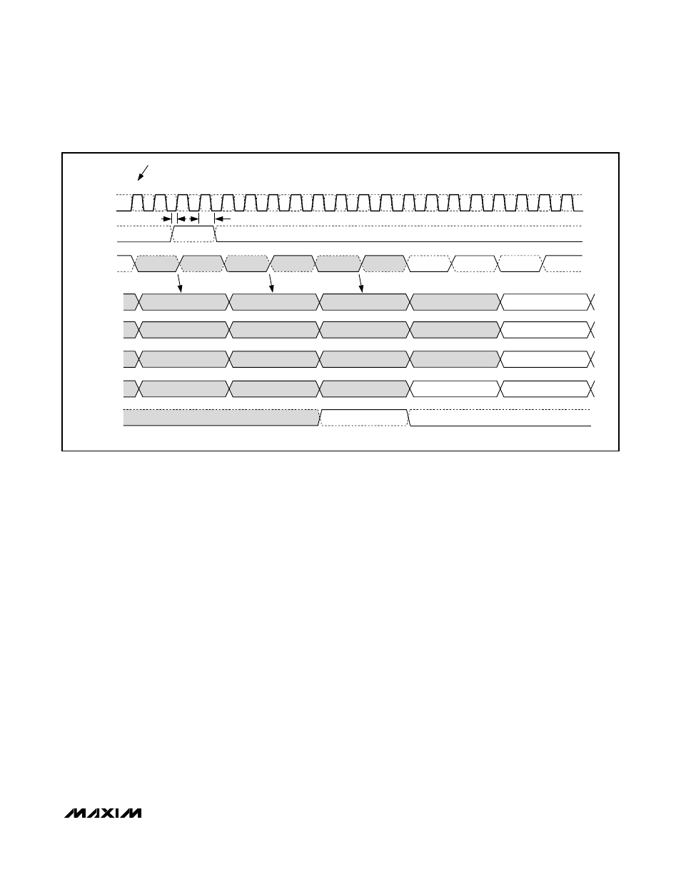
CLKN
CLKP
ADC SAMPLE NUMBER
ADC SAMPLES ON THE RISING EDGE OF CLKP
t
SU
t
HD
DCON
RESET
INPUT
RSTINN
RSTINP
DCOP
PORTA DATA
PORTB DATA
PORTC DATA
PORTD DATA
SAMPLE HERE
RESETOUT
DATA PORT
RSTOUTN
RSTOUTP
THE GRAY AREAS INDICATE A POWER-UP DEPENDENT STATE, WHICH IS UNKNOWN AT THE TIME THE RESET IS BEING ASSERTED.
N
N + 1
N + 2
N + 3
N + 4
N + 5
N + 4
N + 6
N + 5
N + 8
N + 7
N + 6
N + 7
N + 8
N + 9 N + 10 N + 11 N + 12 N + 13 N + 14 N + 15 N + 16 N + 17 N + 18 N + 19
Figure 16. Reset Output Timing in Demultiplexed SDR Mode