Max109, Table 6. driving options for dc-coupled clock, Table 7. demultiplexer and reset operations – Rainbow Electronics MAX109 User Manual
Page 22
MAX109
8-Bit, 2.2Gsps ADC with Track/Hold Amplifier
and 1:4 Demultiplexed LVDS Outputs
22
______________________________________________________________________________________
ble input drive requirements. Each clock input is termi-
nated with an on-chip, laser-trimmed 50Ω resistor to
CLKCOM (clock-termination return). The CLKCOM ter-
mination voltage can be connected anywhere between
ground and -2V for compatibility with standard-ECL drive
levels. The clock inputs are internally buffered with a pre-
amplifier to ensure proper operation of the data convert-
er, even with small-amplitude sine-wave sources. The
MAX109 was designed for single-ended, low-phase
noise sine-wave clock signals with as little as 100mV
amplitude (-10dBm), thereby eliminating the need for an
external ECL clock buffer and its added jitter.
Single-Ended Clock Inputs (Sine-Wave Drive)
Excellent performance is obtained by AC- or DC-cou-
pling a low-phase-noise sine-wave source into a single
clock input (Figure 13a, Table 6). For proper DC bal-
ance, the undriven clock input should be externally
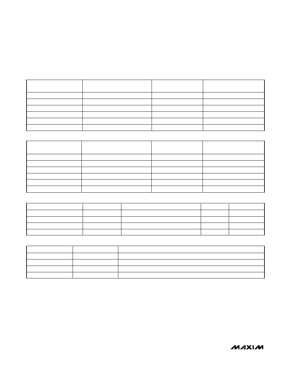
Table 4. Digital Output Codes Corresponding to a DC-Coupled
Single-Ended Analog Input
IN-PHASE/TRUE INPUT
(INP)
INVERTED/COMPLEMENTARY
INPUT (INN)
OUT-OF-RANGE BIT
(DORP/DORN)
OUTPUT CODE
250mV
0
1
11111111 (full scale)
250mV - 1 LSB
0
0
11111111
0
0
0
10000000 toggles 01111111
-250mV + 1 LSB
0
0
00000001
-250mV
0
0
00000000 (zero scale)
<-250mV
0
1
00000000 (out of range)
Table 5. Digital Output Codes Corresponding to a DC-Coupled Differential Analog Input
IN-PHASE/TRUE INPUT
(INP)
INVERTED/COMPLEMENTARY
INPUT (INN)
OUT-OF-RANGE BIT
(DORP/DORN)
OUTPUT CODE
125mV
-125mV
1
11111111 (full scale)
125mV - 0.5 LSB
-125mV + 0.5 LSB
0
11111111
0
0
0
10000000 toggles 01111111
-125mV + 0.5 LSB
125mV - 0.5 LSB
0
00000001
-125mV
125mV
0
00000000 (zero scale)
<-125mV
>+125mV
1
00000000 (out of range)
Table 6. Driving Options for DC-Coupled Clock
CLOCK DRIVE
CLKP
CLKN
CLKCOM
REFERENCE
Single-ended sine wave
-10dBm to +15dBm
Externally terminated to GNDI with 50
Ω
GNDI
Figure 13a
Differential sine wave
-10dBm to +10dBm
-10dBm to +10dBm
GNDI
Figure 13b
Single-ended ECL
ECL drive
-1.3V
-2V
Figure 13c
Differential ECL
ECL drive
ECL drive
-2V
Figure 13d
Table 7. Demultiplexer and Reset Operations
SIGNAL/PIN NAME
TYPE
FUNCTIONAL DESCRIPTION
CLKP/CLKN
Sampling clock inputs
Master ADC timing signal. The ADC samples on the rising edge of CLKP.
DCOP/DCON
LVDS outputs
Data clock output (LVDS). Output data changes on the rising edge of DCOP.
RSTINP/RSTINN
LVDS inputs
D em ul ti p l exer r eset i np ut si g nal s. Resets the i nter nal d em ul ti p l exer w hen asser ted .
RSTOUTP/RSTOUTN
LVDS outputs
Reset outputs for synchronizing the resets of multiple external devices.