Max109 – Rainbow Electronics MAX109 User Manual
Page 3
MAX109
ABSOLUTE MAXIMUM RATINGS
DC ELECTRICAL CHARACTERISTICS
(V
CC
A = V
CC
I = V
CC
D = 5V, V
CC
O = 3.3V, V
EE
= -5V, GNDA = GNDI = GNDO = GNDD = GNDR = 0V, VOSADJ = SAMPADJ =
open, digital output pins differential R
L
= 100Ω. Specifications ≥ +25°C guaranteed by production test, < +25°C guaranteed by
design and characterization. Typical values are at T
A
= +25°C, unless otherwise noted.)
Stresses beyond those listed under “Absolute Maximum Ratings” may cause permanent damage to the device. These are stress ratings only, and functional
operation of the device at these or any other conditions beyond those indicated in the operational sections of the specifications is not implied. Exposure to
absolute maximum rating conditions for extended periods may affect device reliability.
V
CC
A to GNDA ....................................................... -0.3V to +6V
V
CC
D to GNDD ....................................................... -0.3V to +6V
V
CC
I to GNDI ........................................................... -0.3V to +6V
V
CC
O to GNDO ................................................... -0.3V to +3.9V
V
EE
to GNDI ............................................................ -6V to +0.3V
Between Grounds (GNDA, GNDI, GNDO,
GNDD, GNDR) ................................................ -0.3V to +0.3V
V
CC
A to V
CC
D ..................................................... -0.3V to +0.3V
V
CC
A to V
CC
I ....................................................... -0.3V to +0.3V
Differential Voltage between INP and INN ........................... ±1V
INP, INN to GNDI ................................................................. ±1V
Differential Voltage between CLKP and CLKN..................... ±3V
CLKP, CLKN, CLKCOM to GNDI ............................... -3V to +1V
Digital LVDS Outputs to GNDO .............. -0.3V to (V
CC
O - 0.3V)
REFIN, REFOUT to GNDR ........................-0.3V to (V
CC
I + 0.3V)
REFOUT Current ...............................................-100µA to +5mA
RSTINP, RSTINN to GNDA .....................-0.3V to (V
CC
O + 0.3V)
RSTOUTP, RSTOUTN to GNDO .............-0.3V to (V
CC
O + 0.3V)
VOSADJ, SAMPADJ,
TEMPMON to GNDI...............................-0.3V to (V
CC
I + 0.3V)
PRN, DDR, QDR to GNDD.......................-0.3V to (V
CC
D + 0.3V)
DELGATE0, DELGATE1 to GNDA ...........-0.3V to (V
CC
A + 0.3V)
Continuous Power Dissipation (T
A
= +70°C)
256-Ball SBGA (derate 74.1mW/°C above +70°C for
a multilayer board) ................................................. 5925.9mW
Operating Temperature Range
MAX109EHF ...................................................-40°C to +85°C
Thermal Resistance θ
JA
(Note 1) .......................................3°C/W
Operating Junction Temperature.....................................+150°C
Storage Temperature Range .............................-65°C to +150°C
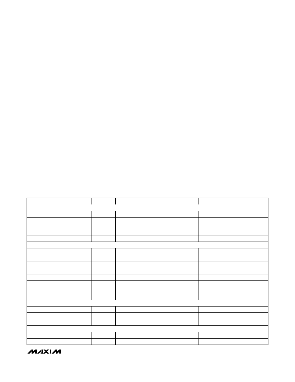
PARAMETER
SYMBOL
CONDITIONS
MIN
TYP
MAX
UNITS
DC ACCURACY
Resolution
RES
8
Bits
Integral Nonlinearity (Note 2)
INL
(Note 8)
-0.8
±0.25
+0.8
LSB
Differential Nonlinearity (Note 2)
DNL
Guaranteed no missing codes, T
A
= +25°C
(Note 8)
-0.8
±0.25
+0.8
LSB
Transfer Curve Offset (Note 2)
V
OS
VOSADJ control input open (Note 8)
-5.5
0
+5.5
LSB
ANALOG INPUTS (INN, INP)
Common-Mode Input-Voltage
Range
V
CM
Signal and offset with respect to GNDI
±1
V
Common-Mode Rejection Ratio
(Note 3)
CMRR
50
dB
Full-Scale Input Range (Note 2)
V
FS
V
REFIN
= 2.5V
470
500
535
mV
P-P
Input Resistance
R
IN
45
50
55
Ω
Input Resistance Temperature
Coefficient
TC
R
150
ppm/°C
VOS ADJUST CONTROL INPUT (VOSADJ)
Input Resistance (Note 4)
R
VOSADJ
25
50
75
k
Ω
VOSADJ = 0V
-20
mV
Input Offset Voltage
V
OS
VOSADJ = 2.5V
20
mV
SAMPLE ADJUST CONTROL INPUT (SAMPADJ)
Input Resistance
R
SAMPADJ
25
50
75
k
Ω
Aperture Time Adjust Range
t
AD
SAMPADJ = 0 to 2.5V
30
ps
8-Bit, 2.2Gsps ADC with Track/Hold Amplifier
and 1:4 Demultiplexed LVDS Outputs
_______________________________________________________________________________________
3
Note 1: Thermal resistance is based on a 5in x 5in multilayer board. The data sheet assumes a thermal environment of 3°C/W.
Thermal resistance may be different depending on airflow and heatsink cooling capabilities.