Max109, Applications information – Rainbow Electronics MAX109 User Manual
Page 21
MAX109
nal shift register is enabled and multiplexed with the
input of the 1:4 demultiplexer, replacing the quantizer
8-bit output. The test pattern consists of 8 bits. Table 3
depicts the composition of the first and last steps of the
PRN pattern. The entire look-up table can be down-
loaded from the Maxim website at www.maxim-ic.com.
Applications Information
Single-Ended Analog Inputs
The MAX109 is designed to work at full speed for both
single-ended and differential analog inputs; however,
for optimum dynamic performance it is recommended
that the inputs are driven differentially. Inputs INP and
INN feature on-chip, laser-trimmed 50Ω termination
resistors.
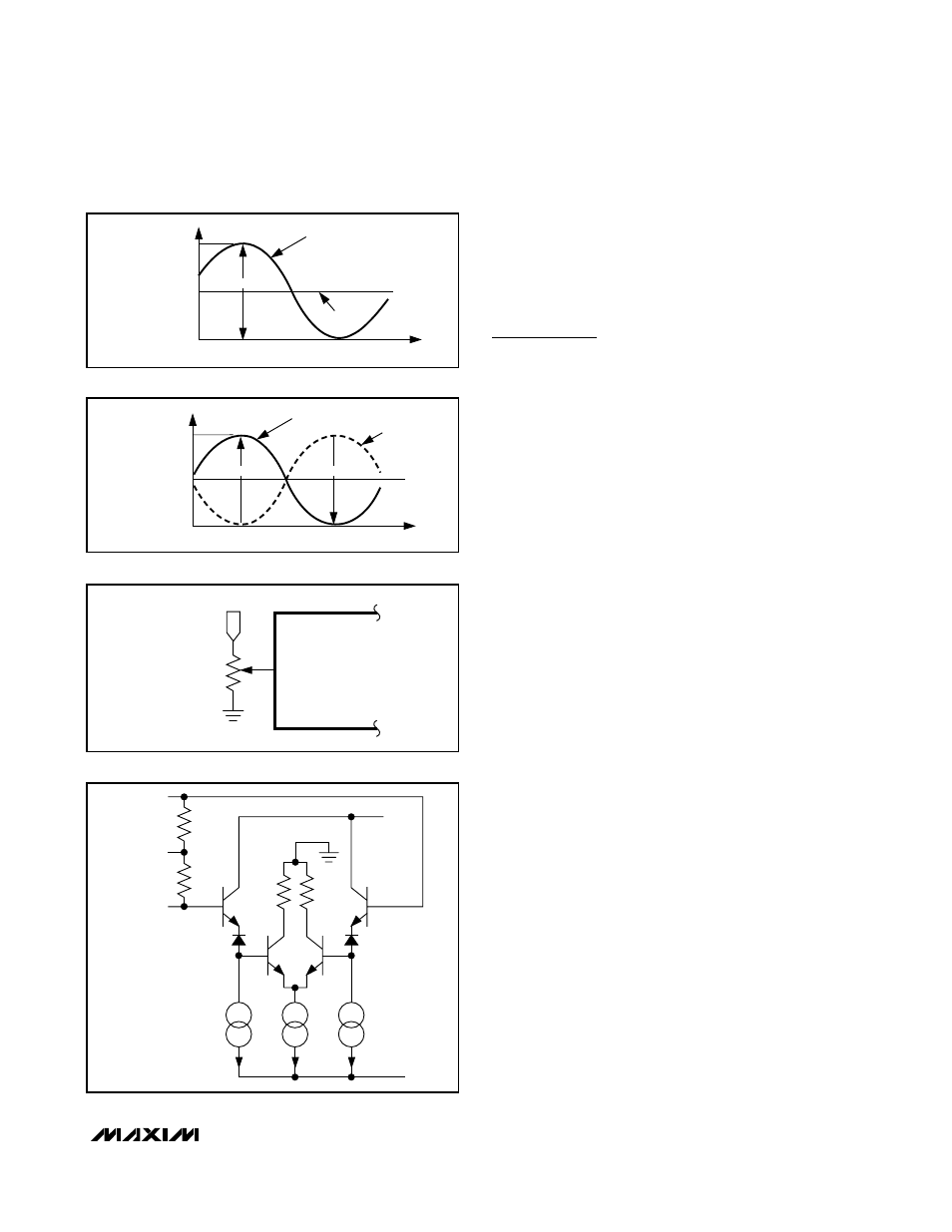
In a typical single-ended configuration, the analog
input signal (Figure 9) enters the T/H amplifier stage at
the in-phase input (INP), while the inverted phase input
(INN) is reverse-terminated to GNDI with an external
50Ω resistor. Single-ended operation allows for an input
amplitude of 500mV
P-P
. Table 4 shows a selection of
input voltages and their corresponding output codes
for single-ended operation.
Differential Analog Inputs
To obtain a full-scale digital output with differential input
drive (Figure 10), 250mV
P-P
must be applied between
INP and INN (INP = 125mV and INN = -125mV). Mid-
scale digital output codes (01111111 or 10000000)
occur when there is no voltage difference between INP
and INN. For a zero-scale digital output code, the in-
phase INP input must see -125mV and the inverted
input INN must see 125mV. A differential input drive is
recommended for best performance. Table 5 repre-
sents a selection of differential input voltages and their
corresponding output codes.
Offset Adjust
The MAX109 provides a control input (VOSADJ) to
compensate for system offsets. The offset adjust input
is a self-biased voltage-divider from the internal 2.5V
precision reference. The nominal open-circuit voltage is
one-half the reference voltage. With an input resistance
(R
VOSADJ
) of typically 50kΩ, VOSADJ can be driven
with an external 10kΩ potentiometer (Figure 11) con-
nected between REFOUT and GNDI to correct for offset
errors. For stabilizing purposes, decouple this output
with a 0.01µF capacitor to GNDI. VOSADJ allows for a
typical offset adjustment of ±10 LSB.
Clock Operation
The MAX109 clock inputs are designed for either sin-
gle-ended or differential operation (Figure 12) with flexi-
8-Bit, 2.2Gsps ADC with Track/Hold Amplifier
and 1:4 Demultiplexed LVDS Outputs
______________________________________________________________________________________
21
INP
INN
0V
+250mV
-250mV
t
500mV
P-P
FS ANALOG
INPUT RANGE
V
IN
= ±250mV
500mV
Figure 9. Single-Ended Analog Input Signal Swing
INP
INN
+125mV
-125mV
t
±250mV
FS ANALOG
INPUT RANGE
0V
250mV
-250mV
Figure 10. Differential Analog Input Signal Swing
GNDI
POTENTIOMETER
10kΩ
REFOUT
VOSADJ
Figure 11. Offset Adjustment Circuit
CLKP
CLKCOM
SIMPLIFIED DIAGRAM
(INPUT ESD PROTECTION
NOT SHOWN).
CLKN
50Ω
1V
50Ω
GNDI
V
EE
Figure 12. Clock Input Structure