Max109 – Rainbow Electronics MAX109 User Manual
Page 17
MAX109
8-Bit, 2.2Gsps ADC with Track/Hold Amplifier
and 1:4 Demultiplexed LVDS Outputs
______________________________________________________________________________________
17
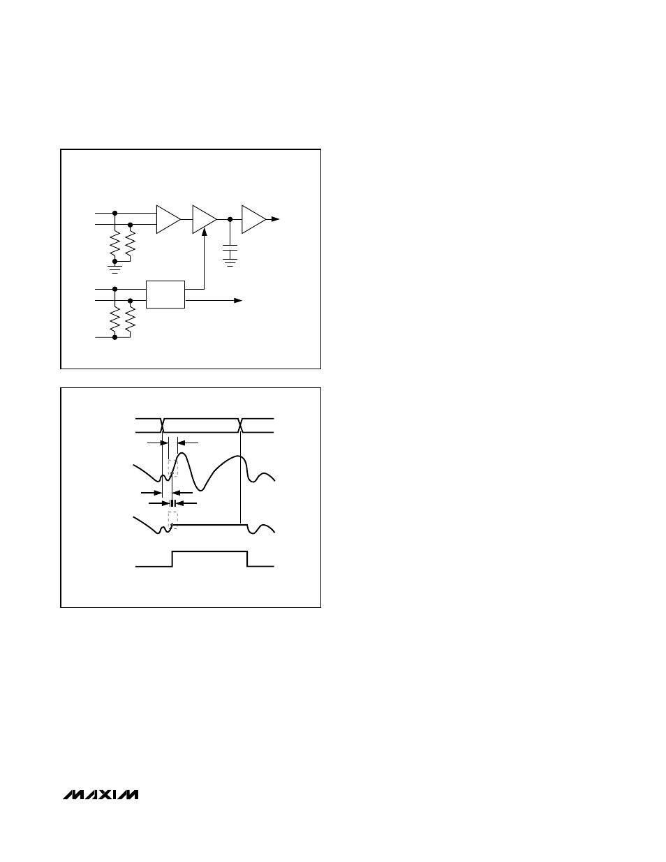
Aperture width, delay, and jitter are parameters that
affect the dynamic performance of high-speed convert-
ers. Aperture jitter, in particular, directly influences SNR
and limits the maximum slew rate (dV/dt) that can be
digitized without contributing significant errors. The
MAX109’s innovative T/H amplifier design limits aper-
ture jitter typically to 0.2ps.
Aperture Width, Aperture Jitter, and Aperture Delay
Aperture width (t
AW
) is the time the T/H circuit requires
to disconnect the hold capacitor from the input circuit
(e.g., to turn off the sampling bridge and put the T/H
unit in hold mode). Aperture jitter (t
AJ
) is the sample-to-
sample variation in the time between the samples.
Aperture delay (t
AD
) is the time defined between the
rising edge of the sampling clock and the instant when
an actual sample event is occurring (Figure 4).
Clock System
The MAX109 clock signals are terminated with 50Ω to
the CLKCOM pin. The clock system provides clock sig-
nals, T/H amplifier, quantizer, and all back-end digital
blocks. The MAX109 also produces a digitized output
clock for synchronization with external FPGA or data-
capture devices. Note that there is a 1.6ns delay
between the clock input (CLKP/CLKN) and its digitized
output representation (DCOP/DCON).
Sampling Point Adjustment (SAMPADJ)
The proper sampling point can be adjusted by utilizing
SAMPADJ as the control line. SAMPADJ accepts an
input-voltage range of 0 to 2.5V, correlating with up to
32ps timing adjustment. The nominal open-circuit volt-
age corresponds to the minimum sampling delay. With
an input resistance R
SAMPADJ
of typically 50kΩ, this
pin can be adjusted externally with a 10kΩ potentiome-
ter connected between REFOUT and GNDI to adjust for
the proper sampling point.
T/H Amplifier to Quantizer Capture Point
Adjustment (DELGATE0, DELGATE1)
Another important feature of the MAX109, is the selec-
tion of the proper quantizer capture point between the
T/H amplifier and the ADC core. Depending on the
selected sampling speed for the application, two con-
trol lines can be utilized to set the proper capture point
between these two circuits. DELGATE0 (LSB) and DEL-
GATE1 (MSB) set the
coarse
timing of the proper cap-
ture point. Using these control lines allow the user to
adjust the time after which the quantizer latches
held
data from the T/H amplifier between 25ps and 50ps
(Table 1). This timing feature enables the MAX109 T/H
amplifier to settle its output properly before the quantiz-
er captures and digitizes the data, thereby achieving
the best dynamic performance for any application.
TO
COMPARATORS
TO
COMPARATORS
BUFFER
AMPLIFIER
INPUT
AMPLIFIER
CLOCK
SPLITTER
SIMPLIFIED DIAGRAM
(INPUT ESD PROTECTION
NOT SHOWN).
GNDI
T/H
50Ω
50Ω
INP
INN
GNDI
C
HOLD
50Ω
50Ω
CLKP
CLKN
CLKCOM
Figure 3. Internal Structure of the 3.2GHz T/H Amplifier
HOLD
CLKP
ANALOG
INPUT
SAMPLED
DATA (T/H)
T/H
t
AW
t
AD
t
AJ
TRACK
TRACK
APERTURE DELAY (t
AD
)
APERTURE WIDTH (t
AW
)
APERTURE JITTER (t
AJ
)
CLKN
Figure 4. T/H Aperture Timing