Electrical characteristics—max1379 (continued), Timing characteristics (figures 6, 10) – Rainbow Electronics MAX1383 User Manual
Page 6
MAX1377/MAX1379/MAX1383
Dual, 12-Bit, 1.25Msps Simultaneous-Sampling
ADCs with Serial Interface
6
_______________________________________________________________________________________
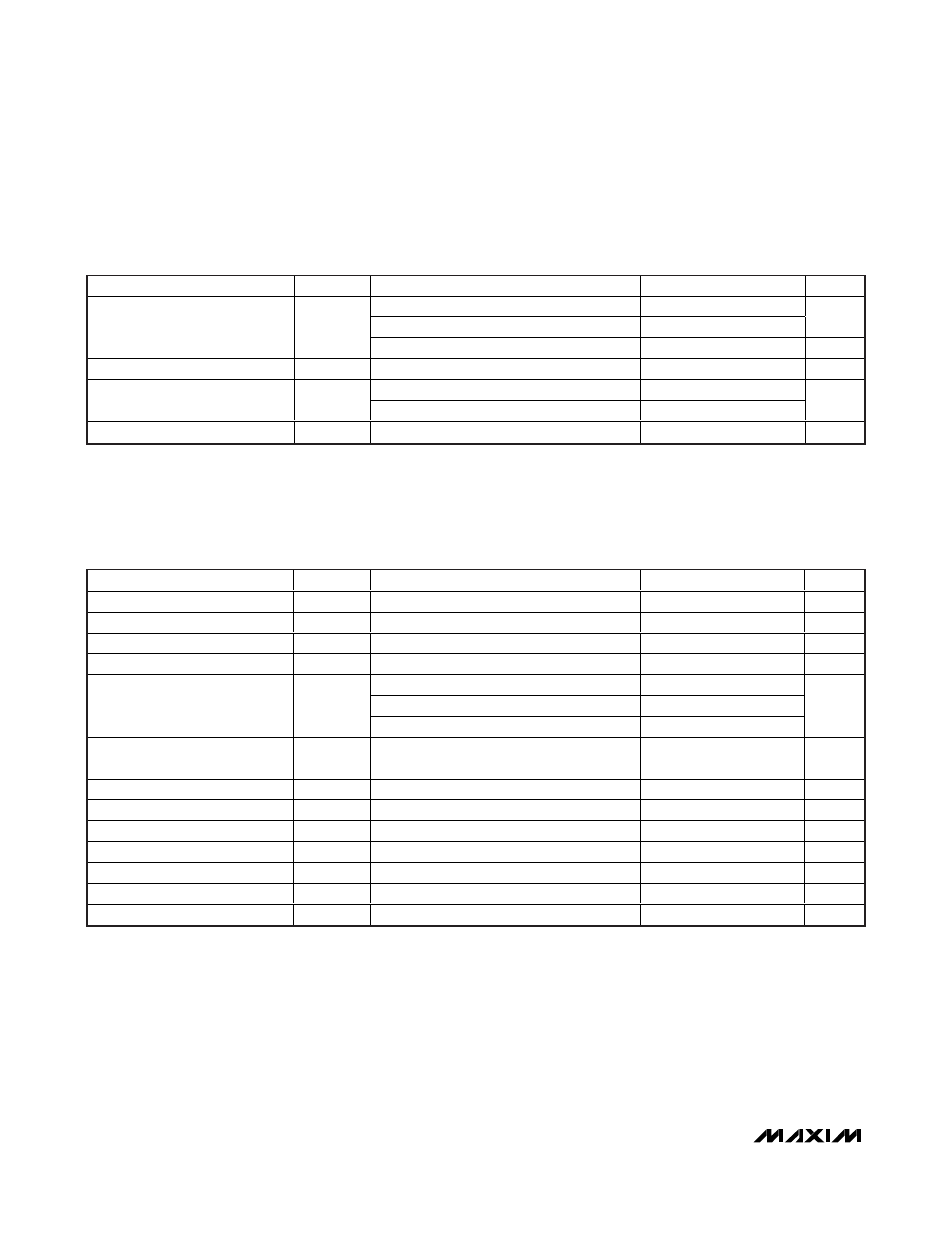
ELECTRICAL CHARACTERISTICS—MAX1379 (continued)
(V
AVDD
= 4.75V to 5.25V, V
L
= 3V, f
SCLK
= 20MHz (50% duty cycle), V
REF
= 4.096V, REFSEL = V
L
, S/
D = DGND, C
REF
= 1µF; T
A
=
T
MIN
to T
MAX
, unless otherwise noted. Typical values are at T
A
= +25°C.)
PARAMETER
SYMBOL
CONDITIONS
MIN
TYP
MAX
UNITS
Normal operation
16
18
Partial power-down mode (Note 5)
2
mA
Analog Supply Current
I
AVDD
Full power-down mode (Note 5)
5
µA
Average Static Current
9
10
mA
f
SCLK
= 20MHz, V
L
= 5V, C
L
= 30pF
2
3
Digital Supply Current
I
VL
f
SCLK
= 20MHz, V
L
= 3V, C
L
= 30pF
1
mA
Power-Supply Rejection
PSR
V
AVDD
= 5V ±10%, full-scale input
±0.2
±3
mV
TIMING CHARACTERISTICS (Figures 6, 10)
V
AVDD
= 4.25V to 5.25V, V
L
= 1.8V to AVDD, V
REF
= 4.096V, f
SCLK
= 20MHz for MAX1379, 50% duty cycle, C
L
= 30pF, T
A
= T
MIN
to
T
MAX
, unless otherwise noted. Typical values are at T
A
= +25°C.)
PARAMETER
SYMBOL
CONDITION
MIN
TYP
MAX
UNITS
SCLK Clock Period
t
CP
50
ns
SCLK Duty Cycle
t
CH
/t
CL
45
55
%
SCLK Pulse-Width High
t
CH
22.5
ns
SCLK Pulse-Width Low
t
CL
22.5
ns
C
L
= 30pF, V
L
= 5V
14
C
L
= 30pF, V
L
= 3V
17
SCLK Rise to DOUT_ Transition
t
DOUT
C
L
= 30pF, V
L
= 1.8V
24
ns
DOUT_ Remains Valid After
SCLK
t
DHOLD
4
ns
CNVST Fall to SCLK Fall
t
SETUP
C
L
= 30pF
10
ns
CNVST Pulse Width
t
CSW
20
ns
Power-Up Time; Full Power-Down
t
PWR-UP
External load on REF < 3µF
2
ms
SEL to CNVST Fall
t
SEL_SETUP
100
120
ns
SEL Hold to CNVST Fall
10
ns
CS Fall To CNVST Fall
t
CST
External load on REF < 3µF
2
ms
Restart Time; Partial Power-Down
t
RCV
No external load
16
Cycles
Note 1: Relative accuracy is the deviation of the analog value at any code from its theoretical value after the gain error and the offset
error have been nulled.
Note 2: Offset nulled.
Note 3: Conversion time is defined as the number of clock cycles (16) multiplied by the clock period. Clock has 50% duty cycle.
Note 4: At sample rates below 10ksps, the input full linear bandwidth is reduced to 5kHz.
Note 5: SCLK and CNVST not switching during measurement.