Detailed description, Input t/h circuit, Input bandwidth – Rainbow Electronics MAX1383 User Manual
Page 12: Analog input protection
MAX1377/MAX1379/MAX1383
Dual, 12-Bit, 1.25Msps Simultaneous-Sampling
ADCs with Serial Interface
12
______________________________________________________________________________________
Detailed Description
The MAX1377/MAX1379/MAX1383 use an input track
and hold (T/H) and SAR circuitry to convert an analog
input signal to a digital 12-bit output. The dual serial
interface requires a minimum of three digital lines
(SCLK, CNVST, and DOUT) and provides easy interfac-
ing to microprocessors (µPs) and DSPs. Four digital
lines are required for dual-output mode.
Input T/H Circuit
Upon power-up, the input T/H circuit enters its tracking
mode immediately. Following a conversion, the T/H
enters the tracking mode on the 14th SCLK rising edge
of the previous conversion (Figure 6). The T/H enters
the hold mode on the falling edge of CNVST. The time
required for the T/H to acquire an input signal is deter-
mined by how quickly the input capacitance is
charged. If the input signal’s source impedance is high,
the acquisition time lengthens. The acquisition time,
t
ACQ
, is the minimum time needed for the signal to be
acquired (see the
Definitions
section). t
ACQ
is calculat-
ed by the following equation:
t
ACQ
≥ 9 x (R
S
+ R
IN
) x C
IN
where R
IN
= 450Ω, C
IN
= 16pF, and R
S
is the source
impedance of the input signal.
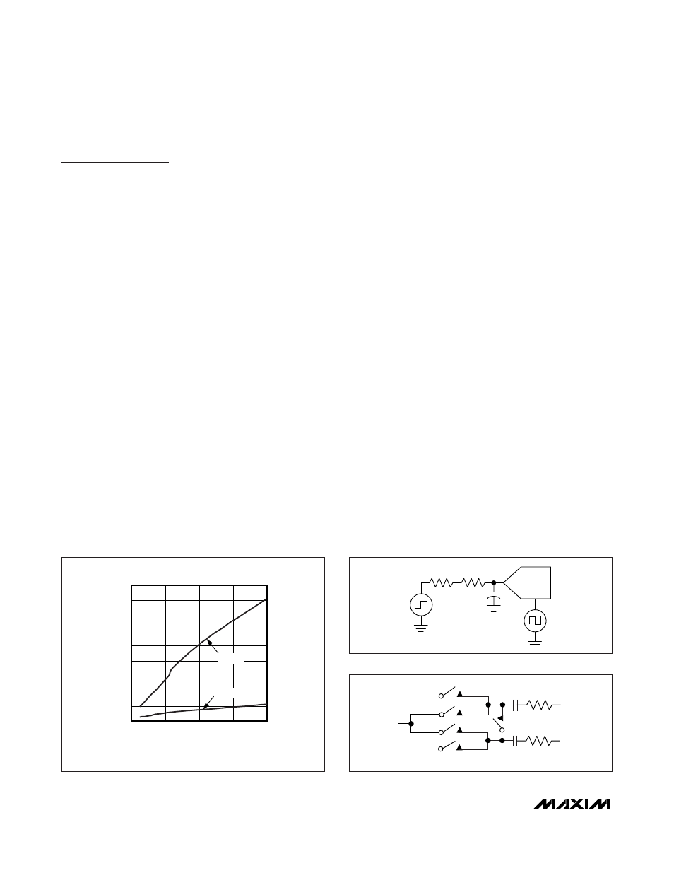
Figure 1 shows the acquisition time as tested using the
circuit of Figure 2. The acquisition time is the time
between the rising edge of a 1V to 3V step input and
the falling edge of CONVST which produced a stable
sample. Rs represents the source impedance of the
function generator (50Ω) and Rx represents the vari-
able filter resistance.
Unipolar Mode
The MAX1377/MAX1379/MAX1383 support two simulta-
neously sampled, single-ended conversions in unipolar
mode. Drive
U/B low for unipolar mode. In unipolar
mode, switches A–D in Figure 3 close according to the
position of SEL. Drive SEL low to close switches A and
D and designate AIN1A and AIN2A as the active, sin-
gle-ended inputs referenced to RGND. Drive SEL high
to close switches B and D and select AIN1B and AIN2B
as the active, single-ended inputs referenced to RGND.
The output code in unipolar mode is straight binary.
See Figure 4 for the unipolar transfer function.
Bipolar Mode
Drive
U/B high to configure the inputs for bipolar/differ-
ential mode. Switches A and C in Figure 3 are closed,
designating AIN1A (AIN2A) and AIN1B (AIN2B) as the
active, differential inputs. In bipolar mode, SEL is
ignored. The output code is in two’s complement.
Figure 5 shows the transfer function for bipolar mode.
Input Bandwidth
The ADC’s input-tracking circuitry has a 5MHz small-
signal bandwidth, allowing the ADC to digitize high-
speed transient events and measure periodic signals
with bandwidths exceeding the ADC’s sampling rate by
using undersampling techniques. To avoid high-fre-
quency signals being aliased into the frequency band
of interest, anti-alias filtering is recommended.
Analog Input Protection
Internal protection diodes that clamp the analog input
to AVDD and AGND allow the analog inputs to swing
from AGND - 0.3V to AVDD + 0.3V without damage to
RGND
A
B
C
D
AIN1A
(AIN2A)
AIN1B
(AIN2B)
C
IN
R
IN
TO ADC+
TO ADC-
C
IN
R
IN
Figure 3. Equivalent Input Circuit
ADC
Rx
Rs
CONVST
C
1V TO 3V
STEP
Figure 2. Test Circuit
M
AX1377 fig01
SOURCE IMPEDANCE, Rx (
Ω)
ACQUISITION TI
M
E (ns)
150
100
50
200
400
600
800
1000
1200
1400
1600
1800
0
0
200
C = 1nF
C = 120pF
Figure 1. Acquisition Time vs. Source Impedance