Pin description – Rainbow Electronics MAX1383 User Manual
Page 11
MAX1377/MAX1379/MAX1383
Dual, 12-Bit, 1.25Msps Simultaneous-Sampling
ADCs with Serial Interface
______________________________________________________________________________________
11
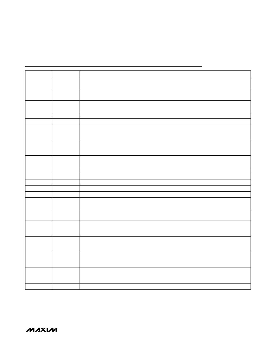
Pin Description
PIN
NAME
FUNCTION
1
REFSEL
Reference-Select Input. Drive REFSEL high to select external reference mode and power down the
internal reference. Drive REFSEL low to select internal reference mode.
2
REF
Internal Reference Output/External Reference Input. For internal reference mode, bypass REF to
RGND with a
≥ 1µF capacitor. For external reference mode, apply a reference voltage at REF.
3
RGND
Reference Ground/Common Negative Input. In bipolar mode, RGND is the reference ground. In
unipolar mode, RGND is the common negative input for all four analog inputs (see Figure 3).
4, 18
AGND
Analog Ground
5
AVDD
Analog-Supply Input. Bypass AVDD with a 10µF || 10nF capacitor to ground.
6
AIN2A
Primary/Positive Analog Input Channel 2. AIN2A is the primary channel 2 input (AIN2A) if using
single-ended inputs (
U/B is low) and the positive channel 2 input (AIN2+) if using differential inputs
(
U/B is high) (see Figure 3).
7
AIN2B
Secondary/Negative Analog Input Channel 2. AIN2B is the secondary channel 2 input (AIN2B) if
using single-ended inputs (
U/B is low) and the negative channel 2 input (AIN2-) if using differential
inputs (
U/B is high) (see Figure 3).
8
U/B
Unipolar/Bipolar Input. Drive
U/B low to select unipolar mode. Drive U/B high to select bipolar
mode. In bipolar mode, the analog inputs are differential.
9
DGND
Digital Supply Ground
10
V
L
Digital Supply Input. Bypass V
L
with a 10µF || 10nF capacitor to ground.
11
DOUT2
Serial-Data Output 2. Data is clocked out on the rising edge of SCLK.
12
DOUT1
Serial-Data Output 1. Data is clocked out on the rising edge of SCLK.
13
SCLK
Serial-Clock Input. Clocks data out of the serial interface. SCLK also sets the conversion time.
14
CNVST
Conversion-Start Input. Forcing CNVST high prepares the device for a conversion. Conversion
begins on the falling edge of CNVST.
15
CS
Active-Low, Chip-Select Input. Drive
CS low to enable the serial interface. When CS is high, DOUT1
and DOUT2 are high impedance, the serial interface resets, and the device powers down.
16
S/
D
Single-Output/Dual-Output Selection Input. Drive S/
D high to route ADC2 data through DOUT1 after
ADC1 data. Drive S/
D low for dual outputs with ADC1 data going to DOUT1 and ADC2 data going
to DOUT2. See the Single-/Dual-Output Modes (S/
D) section.
17
SEL
Analog-Input Selection Input. If
U/B is low (unipolar mode), drive SEL low to select the primary
inputs, AIN1A and AIN2A. Drive SEL high to select the secondary inputs, AIN1B and AIN2B. In
bipolar mode, SEL is ignored.
19
AIN1B
Secondary/Negative Analog Input Channel 1. AIN1B is the secondary channel 1 input (AIN1B) if
using single-ended inputs (
U/B is low) and the negative channel 1 input (AIN1-) if using differential
inputs (
U/B is high) (see Figure 3).
20
AIN1A
Primary/Positive Analog Input Channel 1. AIN1A is the primary channel 1 input (AIN1A) if using
single-ended inputs (
U/B is low) and the positive channel 1 input (AIN1+) if using differential inputs
(
U/B is high) (see Figure 3).
—
EP
Exposed Pad. EP is internally connected to AGND.