Electrical characteristics—max1377 (continued) – Rainbow Electronics MAX1383 User Manual
Page 3
MAX1377/MAX1379/MAX1383
Dual, 12-Bit, 1.25Msps Simultaneous-Sampling
ADCs with Serial Interface
_______________________________________________________________________________________
3
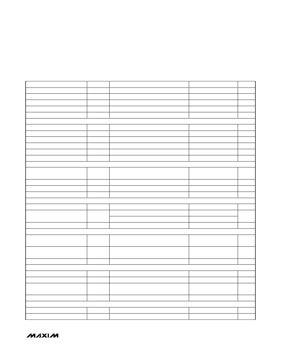
ELECTRICAL CHARACTERISTICS—MAX1377 (continued)
(V
AVDD
= 2.7V to 3.6V, V
L
= 1.8V to AVDD, f
SCLK
= 20MHz (50% duty cycle), V
REF
= 2.048V, REFSEL = V
L
, S/
D = DGND, C
REF
=
1µF; T
A
= T
MIN
to T
MAX
, unless otherwise noted. Typical values are at T
A
= +25°C.)
PARAMETER
SYMBOL
CONDITIONS
MIN
TYP
MAX
UNITS
Track-and-Hold Acquisition Time
t
ACQ
125
ns
Aperture Delay
2
ns
Aperture-Delay Matching
2
ns
Aperture Jitter
(Note 5)
30
ps
External Clock Frequency
f
SCLK
20
MHz
ANALOG INPUTS (AIN1A, AIN1B, AIN2A, AIN2B)
Input Range
U/B = 0, V
AIN_A
- RGND
0
V
REF
V
Differential Input Range
U/B = 1, V
AIN_A
- V
AIN_B
-V
REF
/2
+V
REF
/2
V
Absolute Voltage Range
0
AVDD
V
DC Leakage Current
±1
µA
Input Impedance
34
k
Ω
Input Capacitance
At each analog input
16
pF
EXTERNAL REFERENCE (REFSEL = 1)
Absolute Input Voltage Range
V
REF
1.0
AVDD
+ 0.05
V
Input Capacitance
50
pF
DC Leakage Current
±1
µA
Input Current
Time averaged at maximum throughput rate
800
µA
INTERNAL REFERENCE (REFSEL = 0)
Reference Voltage Level
2.028
2.048
2.068
V
I
SOURCE
= 0 to 1mA
1
Load Regulation
I
SINK
= 0 to 50µA
1
mV/mA
Voltage Temperature Coefficient
±50.0
ppm/
o
C
DIGITAL INPUTS (SCLK, CNVST,
U/B, S/D, SEL, REFSEL)
Input-Voltage Low
V
IL
0.3 x
V
L
V
Input-Voltage High
V
IH
0.7 x
V
L
V
Input Leakage Current
I
IL
±10
µA
DIGITAL OUTPUT (DOUT1, DOUT2)
Output Load Capacitance
C
DOUT
For stated timing performance
30
pF
Output-Voltage Low
V
OL
I
SINK
= 5mA
0.4
V
Output-Voltage High
V
OH
I
SOURCE
= 1mA, V
L
≥ 2.7V
V
L
- 0.5V
V
Output Leakage Current
I
OL
High-impedance mode (Figure 9)
±0.2
µA
POWER REQUIREMENTS
Analog Supply Voltage
AVDD
2.7
3.0
3.6
V
Digital Supply Voltage
V
L
1.8
AVDD
V