Internal reference mode, Input voltage range (max1383), External reference mode – Rainbow Electronics MAX1383 User Manual
Page 13: Serial interface, Initialization after power-up, Starting a conversion and reading the output
MAX1377/MAX1379/MAX1383
Dual, 12-Bit, 1.25Msps Simultaneous-Sampling
ADCs with Serial Interface
______________________________________________________________________________________
13
the MAX1377 and MAX1379. The MAX1383 can handle
±10V input swings. All inputs must not exceed the stat-
ed ranges for accurate conversions.
Internal Reference Mode
Drive REFSEL low to select internal reference mode. The
MAX1377 includes an on-chip 2.048V reference; the
MAX1379 has a 4.096V reference; and the MAX1383
includes a 2.5V internal reference. The reference output
at REF can be used as a reference voltage source for
other components. REF can source up to 2mA. Bypass
REF with a 10nF capacitor and a 4.7µF capacitor to
RGND. It is important to select a low ESR capacitor and
keep the trace resistance as low as possible.
The internal reference is continuously powered-up dur-
ing both normal and partial power-down modes. In full
power-down mode, the internal reference is disabled.
Allow at least 2ms recovery time after a power-on reset
or exiting full power-down mode for the reference to
settle to its intended value.
Input Voltage Range (MAX1383)
The input range on the MAX1383 has an 8x relationship
with the reference voltage. For example, when the refer-
ence voltage (internal or external) is 2.5V, the input
range is ±10V (20V
P-P
).
External Reference Mode
Drive REFSEL high to select external reference mode.
Apply a reference voltage at REF. Bypass REF with
a 10nF capacitor and a 4.7µF capacitor to RGND. As
with the internal reference, it is important to select a low
ESR capacitor and keep the trace resistance as low
as possible.
Serial Interface
Initialization After Power-Up
Upon initial power-up, the MAX1377/MAX1379/ MAX1383
require a complete conversion cycle to initialize the inter-
nal calibration. Following this initialization, the ADC is
ready for normal operation. This initialization is only
required after a hardware power-on reset and is not
required after exiting partial or full power-down mode.
Starting a Conversion and Reading the Output
With SCLK idling high or low, a falling edge on CNVST
begins a conversion (see Figure 6). This causes the
analog input stage to transition from track to hold
mode. SCLK provides the timing for the conversion
process, and data is shifted out as each bit of the result
is determined. A rising edge in CNVST forces the
device into one of three modes. The mode is deter-
mined by the clock cycle in which the transition occurs
and whether the device is set for single or dual outputs.
Figures 7 and 8 show each mode that is activated with
a rising CNVST edge for single and dual outputs.
DOUT1 (and DOUT2, if S/
D = low) transitions from high
impedance to being actively driven low once the ADC
enters hold mode. DOUT_ remains low for the first three
SCLK pulses and begins outputting the conversion result
after the 4th rising edge of SCLK, MSB first. DOUT_ tran-
sitions complete t
DOUT
after each SCLK rising edge and
the DOUT_ values remain valid for t
HOLD
after the next
rising edge of SCLK. A total of 16 SCLK pulses are
required to complete a normal conversion in dual-output
mode and 28 SCLK pulses in single-output mode.
DOUT_ goes low after the 16th rising edge of SCLK and
goes high-impedance when CNVST goes high.
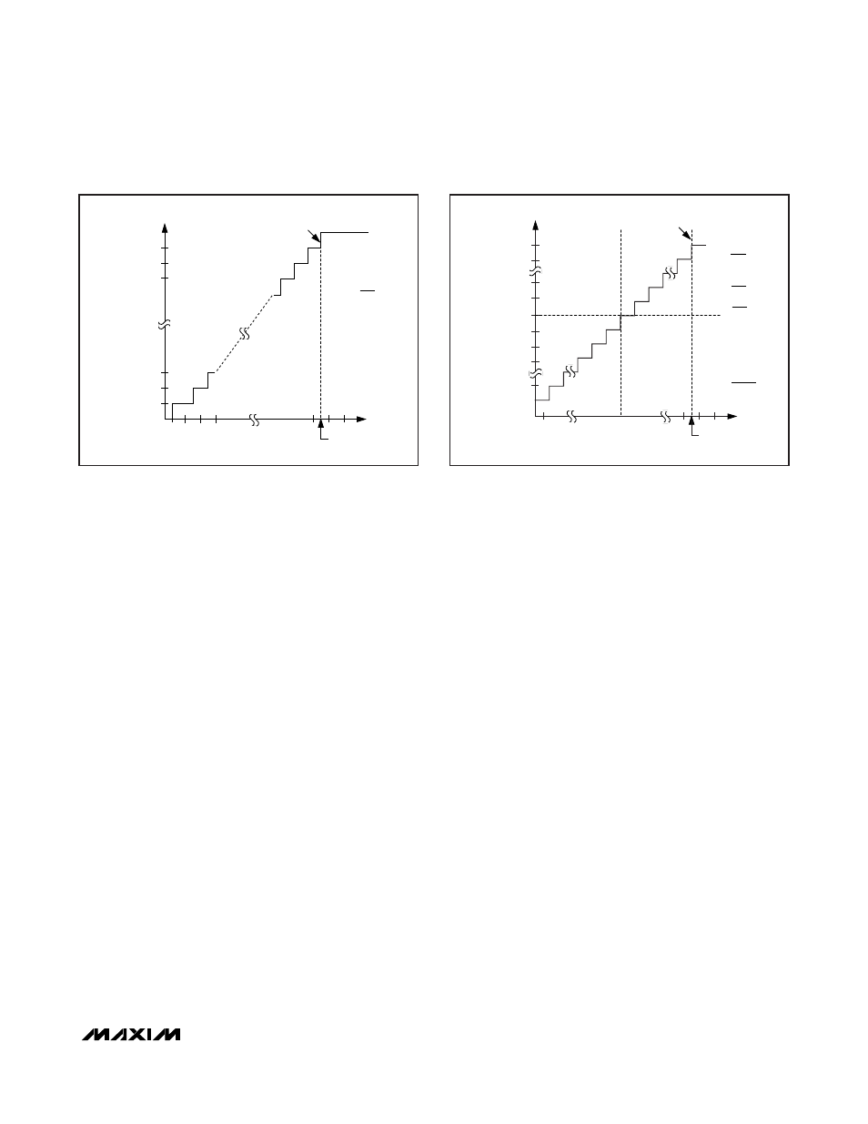
DIGIT
AL OUTPUT CODE
111...111
111...110
000...000
000...001
INPUT VOLTAGE (LSB)
FS
FS - 3/2 LSB
FULL-SCALE
TRANSITION
111...101
000...011
000...010
FS = V
REF
ZS = 0
1 LSB =
V
REF
4096
0
1
2
3
Figure 4. Unipolar Transfer Function (
U/B = Low)
DIGIT
A
L OUTPUT CODE
011...111
011...100
100...000
100...001
DIFFERENTIAL INPUT VOLTAGE (LSB)
+FS
V
REF
- 1 LSB
+FS - 3/2 LSB
FULL-SCALE
TRANSITION
000...000
111...111
111...110
+FS =
V
REF
2
ZS = 0
1 LSB =
V
REF
4096
-FS
000...010
000...001
111...101
-FS =
-V
REF
2
MAX1377/
MAX1379
MAX1383
+FS = 4V
REF
ZS = 0
-FS = -4V
REF
1 LSB =
8 x V
REF
4096
Figure 5. Bipolar Transfer Function (
U/B = High)