Electrical characteristics—max1377 (continued), Electrical characteristics—max1379 – Rainbow Electronics MAX1383 User Manual
Page 4
MAX1377/MAX1379/MAX1383
Dual, 12-Bit, 1.25Msps Simultaneous-Sampling
ADCs with Serial Interface
4
_______________________________________________________________________________________
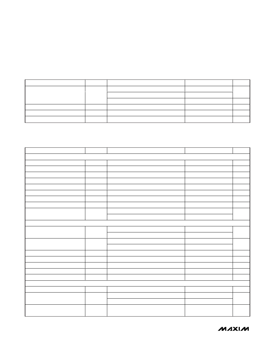
ELECTRICAL CHARACTERISTICS—MAX1377 (continued)
(V
AVDD
= 2.7V to 3.6V, V
L
= 1.8V to AVDD, f
SCLK
= 20MHz (50% duty cycle), V
REF
= 2.048V, REFSEL = V
L
, S/
D = DGND, C
REF
=
1µF; T
A
= T
MIN
to T
MAX
, unless otherwise noted. Typical values are at T
A
= +25°C.)
PARAMETER
SYMBOL
CONDITIONS
MIN
TYP
MAX
UNITS
Normal operation
13
15
Partial power-down mode (Note 5)
2
mA
Analog Supply Current
I
AVDD
Full power-down mode (Note 5)
1
5
µA
Average Static Supply Current
8
10
mA
Digital Supply Current
I
VL
f
SCLK
= 20MHz, V
L
= 3V, C
L
= 30pF
1
1.5
mA
Power-Supply Rejection
PSR
V
AVDD
= 3V ±10%, full-scale input
±0.2
±3
mV
ELECTRICAL CHARACTERISTICS—MAX1379
(V
AVDD
= 4.75V to 5.25V, V
L
= 3V, f
SCLK
= 20MHz (50% duty cycle), V
REF
= 4.096V, REFSEL = V
L
, S/
D = DGND, C
REF
= 1µF; T
A
=
T
MIN
to T
MAX
, unless otherwise noted. Typical values are at T
A
= +25°C.)
PARAMETER
SYMBOL
CONDITIONS
MIN
TYP
MAX
UNITS
DC ACCURACY
Resolution
12
Bits
Relative Accuracy
INL
(Note 1)
-1.25
+1.25
LSB
Differential Nonlinearity
DNL
-1
+1
LSB
Offset Error
±8
LSB
Offset-Error Matching
±9
LSB
Gain Error
(Note 2)
±6
LSB
Gain-Error Matching
(Note 2)
±9
LSB
Gain Temperature Coefficient
±2
ppm/
o
C
AIN1A to AIN1B, AIN2A to AIN2B
80
DC Input Isolation
AIN1A to AIN2A, AIN1B to AIN2B
80
dB
DYNAMIC SPECIFICATIONS (f
IN
= 500kHz , 4V
P-P
sine wave, 1.25Msps, 20MHz f
SCLK
)
Unipolar
69
70
Signal-to-Noise Plus Distortion
SINAD
Bipolar
70
71
dB
Unipolar
70
71
Signal-to-Noise Ratio
SNR
Bipolar
70
72
dB
Total Harmonic Distortion
THD
Up to the 5th harmonic
-84
-76
dB
Spurious-Free Dynamic Range
SFDR
-84
-76
dB
Intermodulation Distortion
IMD
f
IN1
= 103.5kHz, f
IN2
= 113.5kHz
-78
dB
Full-Power Bandwidth
-3dB point
5
MHz
Full-Linear Bandwidth
(S/N + D) > 68dB, 1V input
1
MHz
CONVERSION RATE (Figure 6)
Minimum Conversion Time
t
CONV
16 clock cycles per conversion (Note 3)
0.8
µs
Dual-output mode, S/
D = 0
1.25
Maximum Throughput Rate
Single-output mode, S/
D = 1
0.625
Msps
Minimum Throughput Rate for
Full Bandwidth Signal
(Note 4)
10
ksps