Typical operating characteristics – Rainbow Electronics MAX1326 User Manual
Page 6
INTEGRAL NONLINEARITY
vs. DIGITAL OUTPUT CODE
MAX1316 toc01
DIGITAL OUTPUT CODE
INL (LSB)
12288
8192
4096
-0.75
-0.50
-0.25
0
0.25
0.50
0.75
1.00
-1.00
0
16384
DIFFERENTIAL NONLINEARITY
vs. DIGITAL OUTPUT CODE
MAX1316 toc02
DIGITAL OUTPUT CODE
DNL (LSB)
12288
8192
4096
-0.75
-0.50
-0.25
0
0.25
0.50
0.75
1.00
-1.00
0
16384
ANALOG SUPPLY CURRENT
vs. SUPPLY VOLTAGE
MAX1316 toc03
SUPPLY VOLTAGE (V)
SUPPLY CURRENT (mA)
5.12
5.00
4.87
35
40
45
50
30
4.75
5.25
f
SAMPLE
= 250ksps
ALL 8 CHANNELS
DRIVEN WITH FULL-
SCALE SINE WAVES
ANALOG SUPPLY CURRENT
vs. TEMPERATURE
MAX1316 toc04
TEMPERATURE (
°C)
SUPPLY CURRENT (mA)
60
35
10
-15
35
40
45
50
30
-40
85
f
SAMPLE
=
250ksps
ALL 8 CHANNELS
DRIVEN WITH FULL-
SCALE SINE WAVES
SHUTDOWN CURRENT
vs. SUPPLY VOLTAGE
MAX1316 toc05
SUPPLY VOLTAGE (V)
SHUTDOWN CURRENT (
µ
A)
4.5
3.5
0.2
0.4
0.6
0.8
0
2.5
5.5
ANALOG
SHUTDOWN
CURRENT
DIGITAL
SHUTDOWN
CURRENT
SHUTDOWN CURRENT
vs. TEMPERATURE
MAX1316 toc06
TEMPERATURE (
°C)
SHUTDOWN CURRENT (
µ
A)
60
35
10
-15
0.2
0.4
0.6
0.8
0
-40
85
ANALOG
SHUTDOWN
CURRENT
DIGITAL
SHUTDOWN
CURRENT
MAX1316–MAX1318/MAX1320–MAX1322/MAX1324–MAX1326
8-/4-/2-Channel, 14-Bit, Simultaneous-Sampling ADCs
with ±10V, ±5V, and 0 to +5V Analog Input Ranges
6
_______________________________________________________________________________________
TIMING CHARACTERISTICS (Figures 3, 4, 5, 6 and 7) (Tables 1, 3) (continued)
Note 7:
Shutdown current is measured with analog input floating. The large amplitude of the maximum shutdown current specifi-
cation is due to automatic test equipment limitations.
Note 8:
Defined as the change in positive full scale caused by ±5% variation in the nominal supply voltage.
Note 9:
CONVST must remain low for at least the acquisition period. The maximum acquisition time is limited by internal capacitor
droop.
Note 10:
CS-to-WR and CS-to-RD pins are internally AND together. Setup and hold times do not apply.
Note 11:
Minimum clock frequency is limited only by the internal T/H droop rate. Limit the time between the falling edge of CONVST
to the falling edge of EOLC to a maximum of 0.25ms.
Note 12:
To avoid T/H droop degrading the sampled analog input signals, the first clock pulse should occur within 10µs of the ris-
ing edge of CONVST, and have a minimum clock frequency of 100kHz.
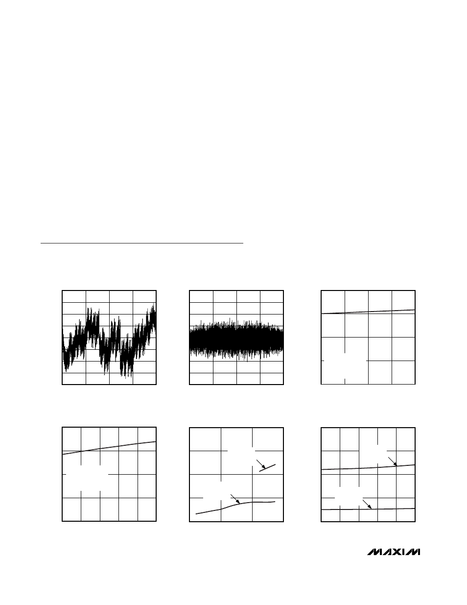
Typical Operating Characteristics
(AV
DD
= +5V, DV
DD
= +3V, AGND = DGND = 0V, V
REF
= V
REFMS
= +2.5V (external reference), see the Typical Operating Circuits sec-
tion, f
CLK
= 10MHz, 50% duty cycle, INTCLK/EXTCLK = AGND (external clock), SHDN = DGND, T
A
= +25°C, unless otherwise noted.)