Rainbow Electronics MAX1326 User Manual
Page 15
MAX1316–MAX1318/MAX1320–MAX1322/MAX1324–MAX1326
8-/4-/2-Channel, 14-Bit, Simultaneous-Sampling ADCs
with ±10V, ±5V, and 0 to +5V Analog Input Ranges
______________________________________________________________________________________
15
Clock Modes
These devices provide an internal clock of 10MHz
(typ). Alternatively, an external clock can be used.
Internal Clock
Internal-clock mode frees the microprocessor from the
burden of running the ADC conversion clock. For internal-
clock operation, connect INTCLK/EXTCLK to AV
DD
and
connect CLK to DGND. Table 1 illustrates the total con-
version time using internal-clock mode.
External Clock
For external-clock operation, connect INTCLK/EXTCLK
to AGND and connect an external-clock source to CLK.
Note that INTCLK/EXTCLK is referenced to the analog
power supply, AV
DD
. The external-clock frequency can
be up to 15MHz, with a duty cycle between 30% and
70%. Clock frequencies of 100kHz and lower can be
used, but the droop in the T/H circuits reduce linearity.
Selecting an Input Buffer
Most applications require an input buffer to achieve 14-
bit accuracy. Although slew-rate and bandwidth are
important, the most critical specification is settling time.
The sampling requires a relatively brief sampling inter-
val of 150ns. At the beginning of the acquisition, the
internal sampling capacitor array connects to CH_ (the
amplifier output), causing some output disturbance.
Ensure the amplifier is capable of settling to at least 14-
bit accuracy during this interval. Use a low-noise, low-
distortion, wideband amplifier (such as the MAX4350 or
MAX4265), which settles quickly and is stable with the
ADC’s capacitive load (in parallel with any bypass
capacitors on the analog inputs).
Applications Section
Digital Interface
The bidirectional, parallel, digital interface sets the 8-bit
configuration register (see the Configuration Register
section) and outputs the 14-bit conversion result. The
interface includes the following control signals: chip
select (CS), read (RD), write (WR), end of conversion
(EOC), end of last conversion (EOLC), convert start
(CONVST), shutdown (SHDN), all on (ALLON), internal-
clock select (INTCLK /EXTCLK), and external-clock input
(CLK). Figures 4, 5, 6, 7, Table 4, and the Timing
Characteristics section show the operation of the inter-
face. D0–D7 are bidirectional, and D8–D13 are output
only. All bits are high impedance when RD = 1 or CS = 1.
Configuration Register
Enable channels as active by writing to the configuration
register through I/O lines D0–D7 (Table 2). The bits in the
configuration register map directly to the channels, with
D0 controlling channel zero, and D7 controlling channel
seven. Setting any bit high activates the corresponding
input channel, while resetting any bit low deactivates the
corresponding channel. Devices with fewer than eight
channels contain some bits that have no function.
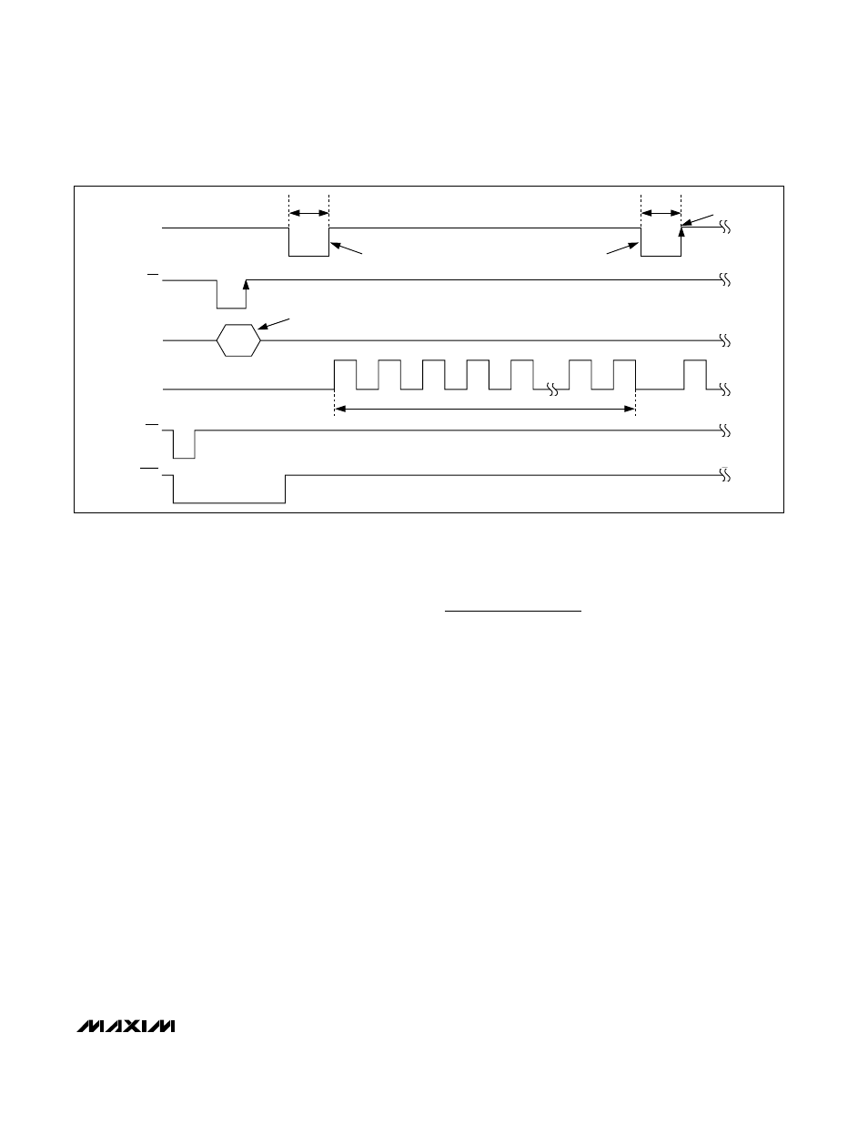
Figure 3. Software Channel Wake-Up Timing (ALLON = 0)
CONVST
D0–D7
CLK
WR
EOC
EOLC
LATCH
t
ACQ
t
ACQ
DUMMY
CONVERSION
START
ACTUAL
CONVERSION
START
DATA-IN
DATA-IN CHANGES ONE OR MORE CHANNELS
FROM POWER-DOWN TO ACTIVE MODE
1
2
3
4
5
14
15
1
>14 CYCLES
SAMPLE