Definitions – Rainbow Electronics MAX1326 User Manual
Page 22
MAX1316–MAX1318/MAX1320–MAX1322/MAX1324–MAX1326
8-/4-/2-Channel, 14-Bit, Simultaneous-Sampling ADCs
with ±10V, ±5V, and 0 to +5V Analog Input Ranges
22
______________________________________________________________________________________
The input range is centered about V
MSV
, which is inter-
nally set to +2.500V. For a custom midscale voltage,
drive REF
MS
with an external voltage source and MSV
will follow REF
MS
. Noise present on MSV or REF
MS
directly couples into the ADC result. Use a precision,
low-drift voltage reference with adequate bypassing to
prevent MSV from degrading ADC performance. For
maximum FSR, be careful not to violate the absolute
maximum voltage ratings of the analog inputs when
choosing V
MSV
. Determine the input voltage as a func-
tion of V
REF
, V
MSV
, and the output code in decimal
using the following equation:
Definitions
Integral Nonlinearity
Integral nonlinearity (INL) is the deviation of the values
on an actual transfer function from a straight line. For
these devices, this straight line is a line drawn between
the end points of the transfer function, once offset and
gain errors have been nullified.
Differential Nonlinearity
Differential nonlinearity (DNL) is the difference between
an actual step width and the ideal value of 1 LSB. For
these devices, the DNL of each digital output code is
measured and the worst-case value is reported in the
Electrical Characteristics table. A DNL error specifica-
tion of less than ±1 LSB guarantees no missing codes
and a monotonic transfer function.
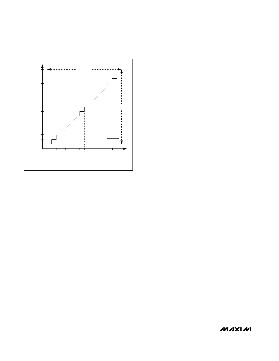
Unipolar Offset Error
For the unipolar MAX1316/MAX1317/MAX1318, the ideal
zero-scale transition from 0x0000 to 0x0001 occurs at
1 LSB (see Figure 11). The unipolar offset error is the
amount of deviation between the measured zero-scale
transition point and the ideal zero-scale transition point.
Bipolar Offset Error
For the bipolar MAX1320/MAX1321/MAX1322/
MAX1324/MAX1325/MAX1326, the ideal zero-point tran-
sition from 0x3FFF to 0x0000 occurs at MSV, which is
usually connected to ground (see Figures 9 and 10).
The bipolar offset error is the amount of deviation
between the measured zero-point transition and the
ideal zero-point transition.
Gain Error
The ideal full-scale transition from 0x1FFE to 0x1FFF
occurs at 1 LSB below full scale (see the Transfer
Functions section). The gain error is the amount of devi-
ation between the measured full-scale transition point
and the ideal full-scale transition point, once offset error
has been nullified.
Signal-to-Noise Ratio
For a waveform perfectly reconstructed from digital
samples, signal-to-noise ratio (SNR) is the ratio of the
full-scale analog input (RMS value) to the RMS quanti-
zation error (residual error). The ideal, theoretical mini-
mum analog-to-digital noise is caused by quantization
noise error only and results directly from the ADC’s res-
olution (N bits):
where N = 14 bits.
In reality, there are other noise sources besides quanti-
zation noise: thermal noise, reference noise, clock jitter,
etc. SNR is computed by taking the ratio of the RMS
signal to the RMS noise, which includes all spectral
components minus the fundamental, the first five har-
monics, and the DC offset.
SNR
N
dB
=
×
+
( .
.
)
6 02
1 76
V
LSB
CODE
V
CH
MSV
_
=
×
+
(
)
10
- 2.500V
Figure 11. 0 to +5V Unipolar Transfer Function
2 x V
REF
2 x V
REF
2 x V
REF
2
14
1 LSB =
BINAR
Y OUTPUT CODE
0
2
16,383
16,381
0x0000
0x0001
0x0002
0x0003
0x3FFF
0x3FFE
0x3FFD
0x3FFC
0x1FFF
0x2000
0x2001
8190
8192
8194
(MSV)
INPUT VOLTAGE (LSBs)