Pin description (continued) – Rainbow Electronics MAX1326 User Manual
Page 10
MAX1316–MAX1318/MAX1320–MAX1322/MAX1324–MAX1326
8-/4-/2-Channel, 14-Bit, Simultaneous-Sampling ADCs
with ±10V, ±5V, and 0 to +5V Analog Input Ranges
10
______________________________________________________________________________________
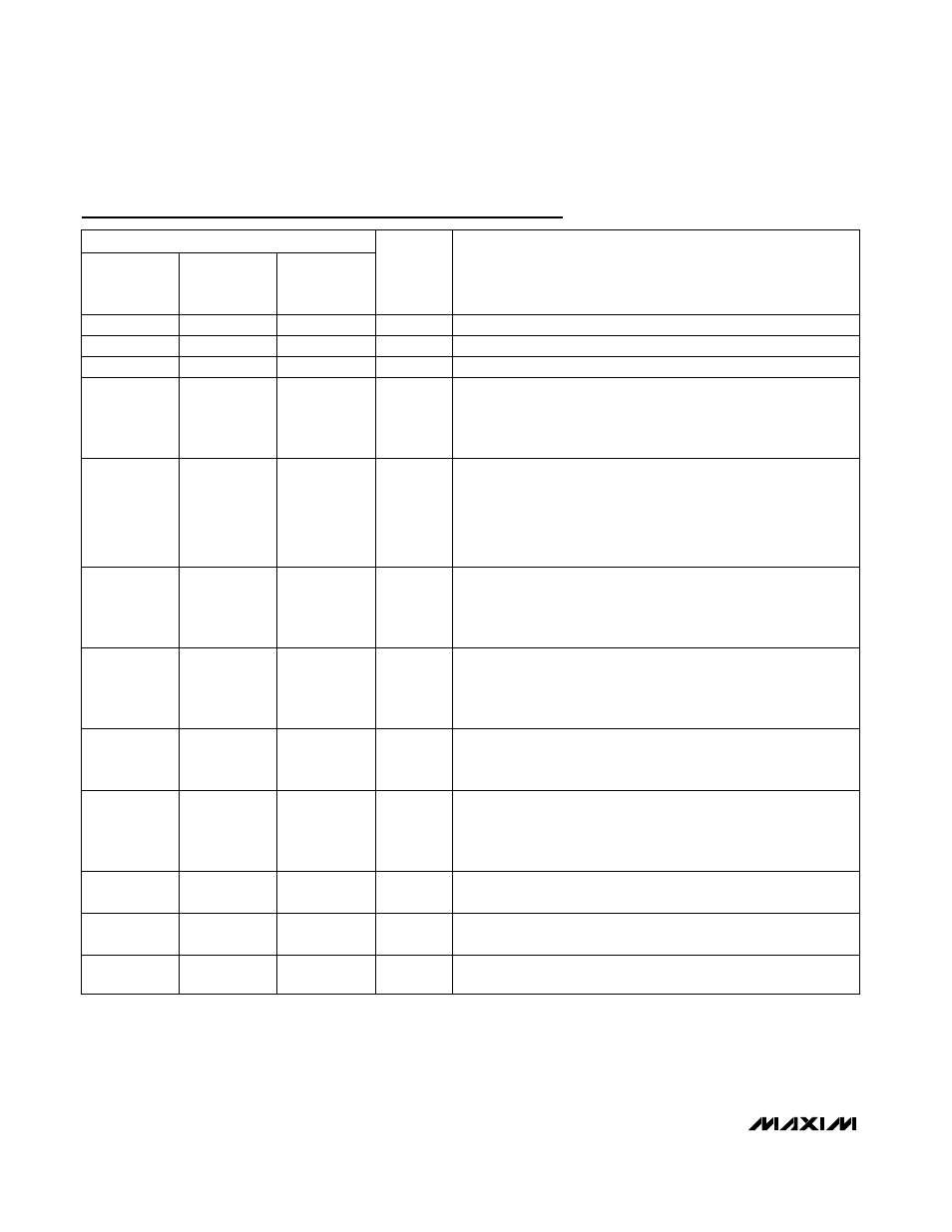
Pin Description (continued)
PIN
MAX1316
MAX1320
MAX1324
MAX1317
MAX1321
MAX1325
MAX1318
MAX1322
MAX1326
NAME
FUNCTION
10
—
—
CH5
Channel 5 Analog Input
11
—
—
CH6
Channel 6 Analog Input
12
—
—
CH7
Channel 7 Analog Input
13
13
13
INTCLK/
EXTCLK
Clock-Mode Select Input. Use INTCLK/EXTCLK to select the internal
or external conversion clock. Connect INTCLK/EXTCLK to AV
DD
to
select the internal clock. Connect INTCLK/EXTCLK to AGND to use
an external clock connected to CLK.
18
18
18
REF
MS
Midscale Reference Bypass or Input. REF
MS
is the bypass point for
an internally generated reference voltage. For the MAX1316/
MAX1317/MAX1318, connect a 0.1µF capacitor from REF
MS
to
AGND. For the MAX1320/MAX1321/MAX1322/MAX1324/
MAX1325/MAX1326, connect REF
MS
directly to REF and bypass
with a 0.1µF capacitor from REF
MS
to AGND.
19
19
19
REF
ADC Reference Bypass or Input. REF is the bypass point for an
internally generated reference voltage. Bypass REF with a 0.01µF
capacitor to AGND. REF can be driven externally by a precision
external voltage reference.
20
20
20
REF+
Positive Reference Bypass. REF+ is the bypass point for an
internally generated reference voltage. Bypass REF+ with a 0.1µF
capacitor to AGND. Also bypass REF+ to REF- with a 2.2µF and a
0.1µF capacitor.
21
21
21
COM
Reference Common Bypass. COM is the bypass point for an
internally generated reference voltage. Bypass COM to AGND with
a 2.2µF and a 0.1µF capacitor.
22
22
22
REF-
Negative Reference Bypass. REF- is the bypass point for an
internally generated reference voltage. Bypass REF- with a 0.1µF
capacitor to AGND. Also bypass REF- to REF+ with a 2.2µF and a
0.1µF capacitor.
24
24
24
D0
Digital I/O Bit 0 of 14-Bit Parallel Data Bus. High impedance when
RD = 1 or CS = 1.
25
25
25
D1
Digital I/O Bit 1 of 14-Bit Parallel Data Bus. High impedance when
RD = 1 or CS = 1.
26
26
26
D2
Digital I/O Bit 2 of 14-Bit Parallel Data Bus. High impedance when
RD = 1 or CS = 1.