Detailed description – Rainbow Electronics MAX1326 User Manual
Page 13
MAX1316–MAX1318/MAX1320–MAX1322/MAX1324–MAX1326
8-/4-/2-Channel, 14-Bit, Simultaneous-Sampling ADCs
with ±10V, ±5V, and 0 to +5V Analog Input Ranges
______________________________________________________________________________________
13
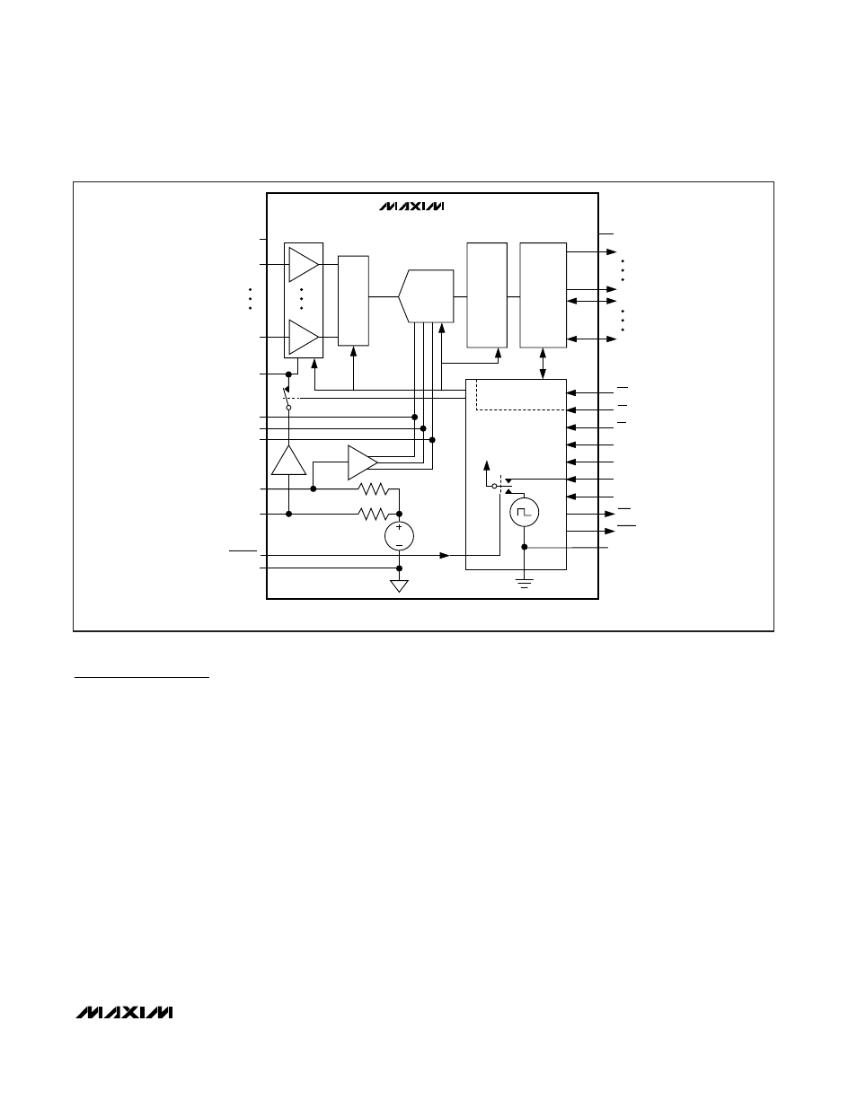
Detailed Description
The MAX1316–MAX1318/MAX1320–MAX1322/MAX1324-
MAX1326 are 14-bit ADCs. They offer two, four, or eight
(independently selectable) input channels, each with its
own T/H circuitry. Simultaneous sampling of all active
channels preserves relative phase information, making
these devices ideal for motor control and power monitor-
ing. These devices are available with 0 to +5V, ±5V, and
±10V input ranges. The 0 to +5V devices feature ±6V
fault-tolerant inputs. The ±5V and ±10V devices feature
±16.5V fault-tolerant inputs. Two channels convert in 2µs;
all eight channels convert in 3.8µs, with a maximum 8-
channel throughput of 263ksps per channel. Internal or
external reference and internal- or external-clock capabil-
ity offer great flexibility and ease of use. A write-only con-
figuration register can mask out unused channels, and a
shutdown feature reduces power. A 16.6MHz, 14-bit, par-
allel data bus outputs the conversion result. Figure 1
shows the functional diagram of these devices.
Analog Inputs
T/H
To preserve phase information across these multichan-
nel devices, each input channel has a dedicated
T/H amplifier.
Use a low-input source impedance to minimize gain-
error harmonic distortion. The time required for the T/H
to acquire an input signal depends on the input source
impedance. If the input signal’s source impedance is
high, the acquisition time lengthens and more time
must be allowed between conversions. The acquisition
time (t
1
) is the maximum time the device takes to
acquire the signal. Use the following formula to calcu-
late acquisition time:
t
1
= 10 (R
S
+ R
IN
) x 6pF
where R
IN
= 2.2k
Ω, R
S
= the input signal’s source
impedance, and t
1
is never less than 180ns. A source
impedance of less than 100
Ω does not significantly
affect the ADC’s performance.
Figure 1. Functional Diagram
MAX1316–MAX1318
MAX1320–MAX1322
MAX1324–MAX1326
CONVST
D13
MSV
DGND
AV
DD
SHDN
CLK
CH0
INTERFACE
AND
CONTROL
8 x 1
MUX
14-BIT
ADC
CH7
D0
DV
DD
AGND
ALLON
REF
MS
REF
REF+
COM
REF-
S/H
S/H
8 x 14
SRAM
OUTPUT
DRIVERS
5k
Ω
5k
Ω
CONFIGURATION
REGISTER
D7
D8
2.500V
*
*SWITCH CLOSED ON UNIPOLAR DEVICES, OPEN ON BIPOLAR DEVICES
INTCLK/EXTCLK
WR
CS
RD
EOC
EOLC