Table 4. reference bypass capacitors – Rainbow Electronics MAX1326 User Manual
Page 19
MAX1316–MAX1318/MAX1320–MAX1322/MAX1324–MAX1326
8-/4-/2-Channel, 14-Bit, Simultaneous-Sampling ADCs
with ±10V, ±5V, and 0 to +5V Analog Input Ranges
______________________________________________________________________________________
19
Reading After Conversion
Figure 7 shows the interface signals for a read operation
after a conversion with all eight channels enabled. At the
falling edge of EOLC, on the 38th clock pulse after the ini-
tiation of a conversion, driving CS and RD low places the
first conversion result onto the parallel bus, which can be
latched on the rising edge of RD. Successive low pulses
of RD place the successive conversion results onto the
bus. Pulse CONVST low to initiate a new conversion.
Power-Up Reset
At power-up, all channels are selected for conversion
(see the Configuration Register section). After applying
power, allow a 1.0ms wake-up time to elapse before ini-
tiating the first conversion. Then, hold CONVST high for
at least 2.0µs after the wake-up time is complete. If
using an external clock, apply 20 clock pulses to CLK
with CONVST high before initiating the first conversion.
Reference
Internal Reference
The internal-reference circuits provide for analog input
voltages of 0 to +5V unipolar (MAX1316/MAX1317/
MAX1318), ±5V bipolar (MAX1320/MAX1321/MAX1322),
or ±10V bipolar (MAX1324/MAX1325/MAX1326). Install
external capacitors for reference stability, as indicated in
Table 4, and as shown in the Typical Operating Circuits.
External Reference
Connect a +2.0V to +3.0V external reference at REF
MS
and/or REF. When connecting an external reference, the
input impedance is typically 5k
Ω. The external reference
must be able to drive 200µA of current and have a low
output impedance. For more information about using
external references see the Transfer Functions section.
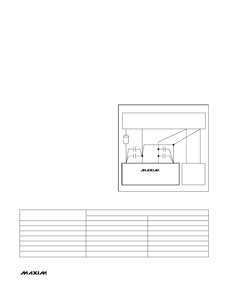
Layout, Grounding, and Bypassing
For best performance use PC boards with ground
planes. Board layout should ensure that digital and
analog signal lines are separated from each other. Do
not run analog and digital lines parallel to one another
(especially clock lines), or do not run digital lines
underneath the ADC package. Figure 8 shows the rec-
ommended system ground connections when not using
a ground plane. A single-point analog ground (star
ground point) should be established at AGND, sepa-
rate from the logic ground. All other analog grounds
and DGND should be connected to this ground.
Figure 8. Power-Supply Grounding and Bypassing
Table 4. Reference Bypass Capacitors
INPUT VOLTAGE RANGE
LOCATION
UNIPOLAR (µF)
BIPOLAR (µF)
MSV bypass capacitor to AGND
2.2 || 0.1
NA
REF
MS
bypass capacitor to AGND
0.01
0.01 (connect REF
MS
to REF)
REF bypass capacitor to AGND
0.01
0.01 (connect REF
MS
to REF)
REF+ bypass capacitor to AGND
0.1
0.1
REF+ to REF- capacitor
2.2 || 0.1
2.2 || 0.1
REF- bypass capacitor to AGND
0.1
0.1
COM bypass capacitor to AGND
2.2 || 0.1
2.2 || 0.1
NA = Not applicable (connect MSV directly to AGND).
SUPPLIES
AV
DD
AGND
DGND
V
DD
DIGITAL
CIRCUITRY
OPTIONAL
FERRITE
BEAD
+5V
RETURN
RETURN
+3V TO +5V
DV
DD
GND
MAX1316–MAX1318
MAX1320–MAX1322
MAX1324–MAX1326