Table 6. ±5v bipolar code table, Table 7. 0 to +5v unipolar code table – Rainbow Electronics MAX1326 User Manual
Page 21
MAX1316–MAX1318/MAX1320–MAX1322/MAX1324–MAX1326
8-/4-/2-Channel, 14-Bit, Simultaneous-Sampling ADCs
with ±10V, ±5V, and 0 to +5V Analog Input Ranges
______________________________________________________________________________________
21
The input range is centered about V
MSV
. Normally,
MSV = AGND, and the input is symmetrical about zero.
For a custom midscale voltage, drive MSV with an
external voltage source. Noise present on MSV directly
couples into the ADC result. Use a precision, low-drift
voltage reference with adequate bypassing to prevent
MSV from degrading ADC performance. For maximum
FSR, be careful not to violate the absolute maximum
voltage ratings of the analog inputs when choosing
V
MSV
. Determine the input voltage as a function of
V
REF
, V
MSV
, and the output code in decimal using the
following equation:
Unipolar 0 to +5V Devices
Table 7 and Figure 11 show the offset binary transfer
function for the MAX1316/MAX1317/MAX1318 with a 0
to +5V input range. The FSR is two times the voltage at
REF. The internal +2.500V reference gives a +5V FSR,
while an external +2V to +3V reference allows an FSR
of +4V to +6V, respectively. Calculate the LSB size
using the following equation:
This equals 0.3052mV when using the internal reference.
LSB
V
REF
=
×
2
2
14
V
LSB
CODE
V
CH
MSV
_
=
×
+
10
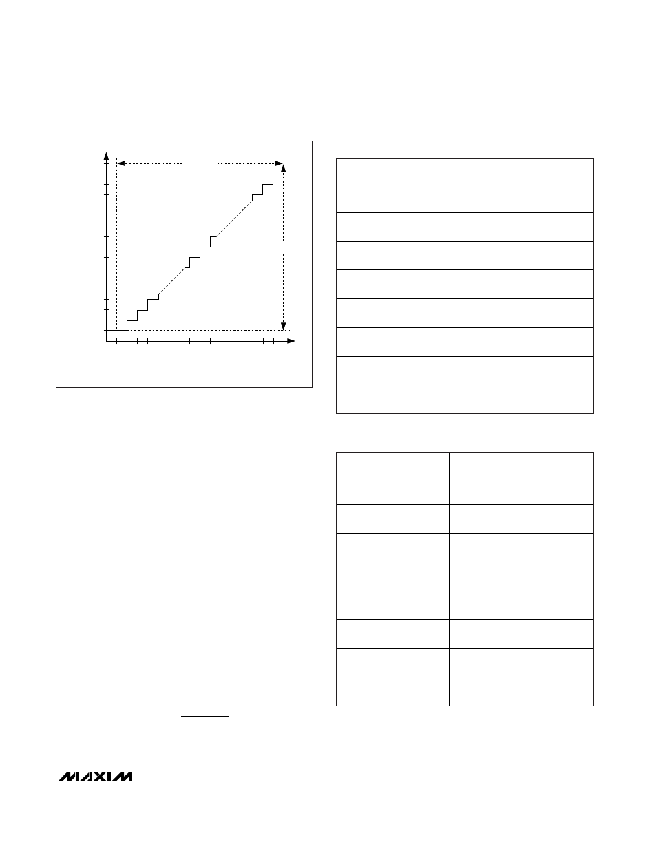
Figure 10. ±5V Bipolar Transfer Function
4 x V
REF
4 x V
REF
4 x V
REF
2
14
1 LSB =
TWO'S COMPLEMENT BINAR
Y OUTPUT CODE
-8192 -8190
+8191
+8189
0x2000
0x2001
0x2002
0x2003
0x1FFF
0x1FFE
0x1FFD
0x1FFC
0x3FFF
0x0000
0x0001
-1 0 +1
(MSV)
INPUT VOLTAGE (V
CH_
- V
MSV
IN LSBs)
Table 6. ±5V Bipolar Code Table
TWO’S COMPLEMENT
BINARY OUTPUT CODE
DECIMAL
EQUIVALENT
OUTPUT
(CODE
10
)
INPUT
VOLTAGE (V)
(V
REF
= 2.5V,
V
MSV
= 0V)
01 1111 1111 1111
0x1FFF
8191
4.9997
±0.5 LSB
01 1111 1111 1110
0x1FFE
8190
4.9991
±0.5 LSB
00 0000 0000 0001
0x0001
1
0.0009
±0.5 LSB
00 0000 0000 0000
0x0000
0
0.0003
±0.5 LSB
11 1111 1111 1111
0x3FFF
-1
-0.0003
±0.5 LSB
10 0000 0000 0001
0x2001
-8191
-4.9991
±0.5 LSB
10 0000 0000 0000
0x2000
-8192
-4.9997
±0.5 LSB
Table 7. 0 to +5V Unipolar Code Table
BINARY OUTPUT CODE
DECIMAL
EQUIVALENT
OUTPUT
(CODE
10
)
INPUT
VOLTAGE (V)
(V
REF
= V
REFMS
= 2.5V)
11 1111 1111 1111
0x3FFF
16383
4.9998
±0.5 LSB
11 1111 1111 1110
0x3FFE
16382
4.9995
±0.5 LSB
10 0000 0000 0001
0x2001
8193
2.5005
±0.5 LSB
10 0000 0000 0000
0x2000
8192
2.5002
±0.5 LSB
01 1111 1111 1111
0x1FFF
8191
2.4998
±0.5 LSB
00 0000 0000 0001
0x0001
1
0.0005
±0.5 LSB
00 0000 0000 0000
0x0000
0
0.0002
±0.5 LSB