Electrical characteristics (continued) – Rainbow Electronics MAX1855 User Manual
Page 6
MAX1716/MAX1854/MAX1855
High-Speed, Adjustable, Synchronous Step-Down
Controllers with Integrated Voltage Positioning
6
_______________________________________________________________________________________
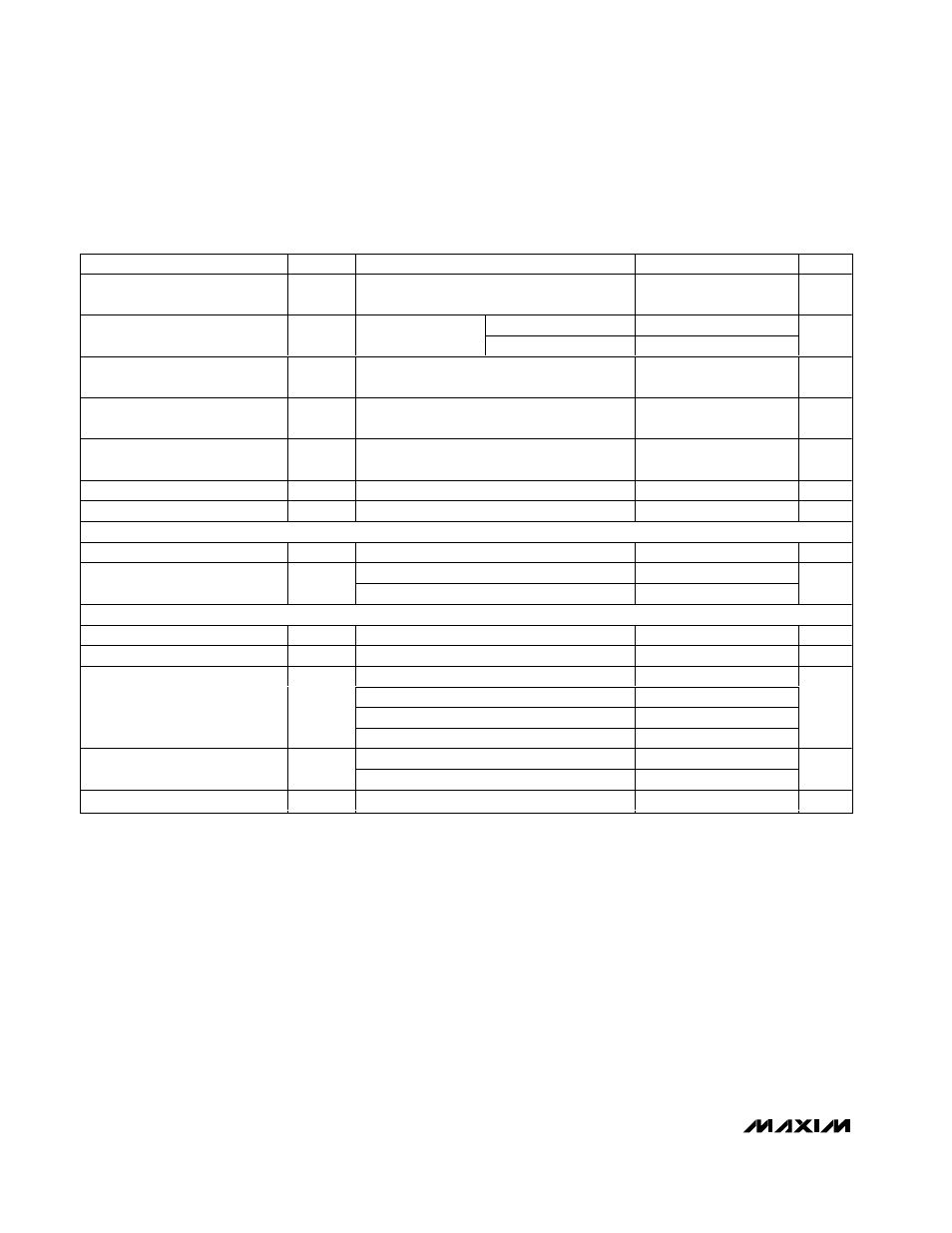
Note 2: Output voltage accuracy specifications apply to DAC voltages from 0.6V to 2.0V. Includes load-regulation error.
Note 3: When the inductor is in continuous conduction, the output voltage will have a DC regulation level higher than the error-com-
parator threshold by 50% of the ripple. In discontinuous conduction (SKIP = GND, light load), the output voltage will have a
DC regulation level higher than the trip level by approximately 1.5% due to slope compensation.
Note 4: On-time and off-time specifications are measured from 50% to 50% at the DH pin, with LX forced to 0, BST forced to 5V, and
a 500pF capacitor from DH to LX to simulate external MOSFET gate capacitance. Actual in-circuit times may be different
due to MOSFET switching speeds.
Note 5: The MAX1854 does not have overvoltage protection.
Note 6: Specifications to -40°C are guaranteed by design, not production tested.
ELECTRICAL CHARACTERISTICS (continued)
(Circuit of Figure 1, V+ = +15V, V
CC
= V
DD
= 5V, SKIP = V
CC
, VPS = PGND, T
A
= -40°C to +85°C, unless otherwise noted.) (Note 6)
PARAMETER
SYMBOL
CONDITIONS
MIN
TYP
MAX
UNITS
Current-Limit Threshold
(Positive, Default)
V
ITH
V
PGND
- V
CS
, ILIM = V
CC
100
140
mV
V
ILIM
= 0.5V
35
65
Current-Limit Threshold
(Positive, Adjustable)
V
ITH
V
PGND
- V
CS
V
ILIM
= 2V (REF)
160
240
mV
V
CC
Undervoltage Lockout
Threshold
Rising edge, hysteresis = 20mV, switching
disabled below this level
4.0
4.45
V
VGATE Lower Trip Threshold
Measured at FB with respect to unloaded
output voltage, falling edge
-12.5
-7.5
%
VGATE Upper Trip Threshold
Measured at FB with respect to unloaded
output voltage, rising edge
7.5
12.5
%
VGATE Output Low Voltage
I
SINK
= 1mA
0.4
V
VGATE Leakage Current
High state, forced to 5.5V
1
µA
GATE DRIVERS
DH Gate Driver On-Resistance
R
ON ( D H )
V
BST
- V
LX
forced to 5V
5
Ω
High state (pullup)
5
DL Gate Driver On-Resistance
R
ON(DL)
Low state (pulldown)
1.7
Ω
LOGIC AND I/O
Logic Input High Voltage
V
IH
D0
−D4, SHDN, SKIP
2.4
V
Logic Input Low Voltage
V
IL
D0
−D4, SHDN, SKIP
0.8
V
TON = V
CC
(200kHz operation)
V
CC
- 0.4
TON = open (300kHz operation)
3.15
3.85
TON = REF (400kHz operation)
1.65
2.35
TON Input Levels
TON = GND (550kHz operation)
0.5
V
TON = GND or V
CC
-3
3
Logic Input Current
SHDN, SKIP = GND or V
CC
-1
1
µA
D0
−D4 Pullup Current
D0
−D4 = GND
3
10
µA