Rainbow Electronics MAX1855 User Manual
Page 17
MAX1716/MAX1854/MAX1855
High-Speed, Adjustable, Synchronous Step-Down
Controllers with Integrated Voltage Positioning
______________________________________________________________________________________
17
switching frequency. The on-time guaranteed in the
Electrical Characteristics table is influenced by switch-
ing delays in the external high-side MOSFET. Resistive
losses—including the inductor, both MOSFETs, output
capacitor ESR, and PC board copper losses in the out-
put and ground—tend to raise the switching frequency
at higher output currents. Switch dead-time can
increase the effective on-time, reducing the switching
frequency. This effect occurs only in PWM mode (SKIP
= high) when the inductor current reverses at light or
negative load currents. With reversed inductor current,
the inductor’s EMF causes LX to go high earlier than
normal, extending the on-time by a period equal to the
DH-rising dead-time.
When the controller operates in continuous mode, the
dead-time is no longer a factor and the actual switching
frequency is:
ƒ = (V
OUT
+ V
DROP1
) / [t
ON
× (V+ + V
DROP1
– V
DROP2
)]
where V
DROP1
is the sum of the parasitic voltage drops
in the inductor discharge path, including synchronous
rectifier, inductor, and PC board resistances; V
DROP2
is
the sum of the resistances in the charging path, includ-
ing high-side switch, inductor, and PC board resis-
tances; and t
ON
is the on-time calculated by the
MAX1716/MAX1854/MAX1855.
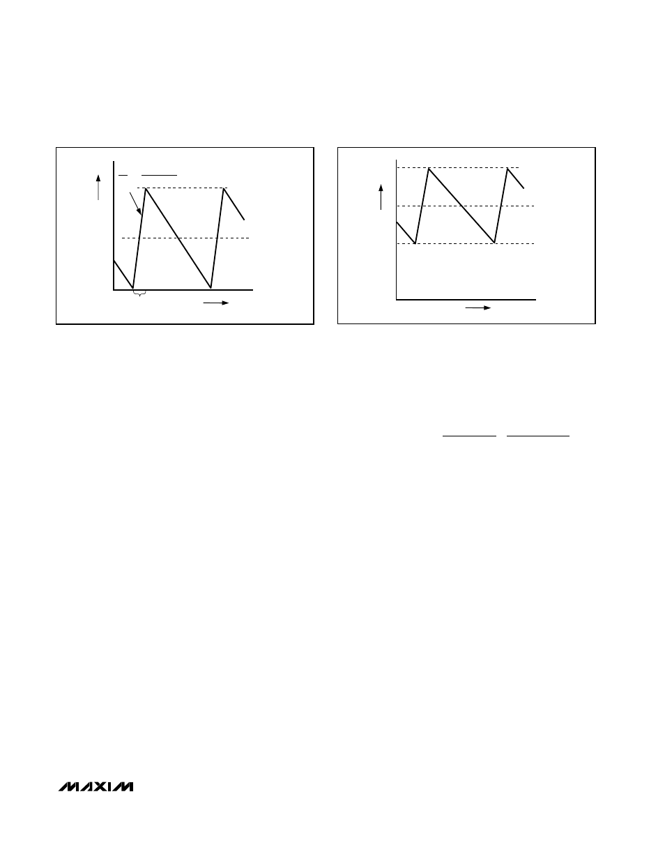
Automatic Pulse-Skipping Switchover
In skip mode (SKIP = low), an inherent automatic
switchover to PFM takes place at light loads (Figure 3).
This switchover is controlled by a comparator that trun-
cates the low-side switch on-time at the inductor cur-
rent’s zero crossing. This mechanism causes the
threshold between pulse-skipping PFM and nonskip-
ping PWM operation to coincide with the boundary
between continuous and discontinuous inductor-cur-
rent operation. For an input voltage (V+) range of 7V to
24V, this threshold is relatively constant, with only a
minor dependence on the input voltage:
where K is the on-time scale factor (Table 3). The load-
current level at which PFM/PWM crossover occurs,
I
LOAD(SKIP)
, is equal to 1/2 the peak-to-peak ripple cur-
rent, which is a function of the inductor value (Figure 3).
For example, in the standard application circuit with
K = 3.3µs (300kHz), V
BATT
= 12V, V
OUT
= 1.6V, and
L = 0.68µH, switchover to pulse-skipping operation
occurs at I
LOAD
= 2.3A or about 1/4 full load. The
crossover point occurs at an even lower value if a
swinging (soft-saturation) inductor is used.
The switching waveforms may appear noisy and asyn-
chronous when light loading causes pulse-skipping
operation; this is a normal operating condition that
improves light-load efficiency. Trade-offs in PFM noise
vs. light-load efficiency are made by varying the induc-
tor value. Generally, low inductor values produce a
broader efficiency vs. load curve, while higher values
result in higher full-load efficiency (assuming that the
coil resistance remains fixed) and less output voltage
ripple. Penalties for using higher inductor values
include larger physical size and degraded load-tran-
sient response (especially at low input voltage levels).
Forced-PWM Mode (
S
SK
KIIP
P
= High)
The low-noise, forced-PWM mode (SKIP driven high)
disables the zero-crossing comparator that controls the
INDUCTOR CURRENT
I
LIMIT
I
LOAD
0
TIME
-I
PEAK
Figure 4. “Valley” Current-Limit Threshold Point
INDUCTOR CURRENT
I
LOAD
= I
PEAK
/2
ON-TIME
0
TIME
-I
PEAK
L
V
BATT
- V
OUT
∆i
∆t
=
Figure 3. Pulse-Skipping/Discontinuous Crossover Point
I
K
V
L
V
V
V
LOAD SKIP
OUT
OUT
(
)
≈
Ч
+ −
+
2