Rainbow Electronics MAX1855 User Manual
Page 2
MAX1716/MAX1854/MAX1855
High-Speed, Adjustable, Synchronous Step-Down
Controllers with Integrated Voltage Positioning
2
_______________________________________________________________________________________
ABSOLUTE MAXIMUM RATINGS
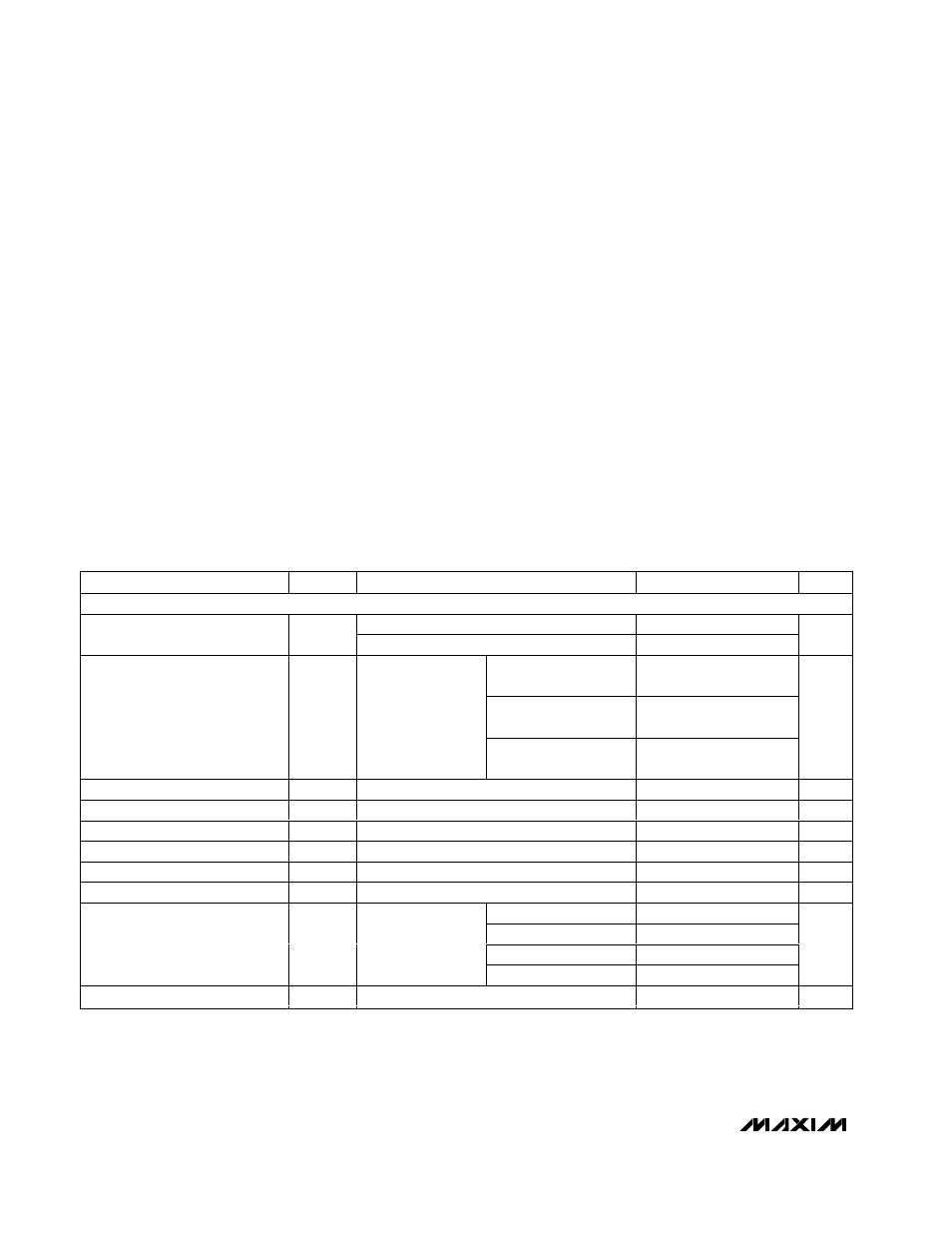
ELECTRICAL CHARACTERISTICS
(Circuit of Figure 1, V+ = +15V, V
CC
= V
DD
= 5V, SKIP = V
CC
, VPS = PGND, T
A
= 0°C to +85°C, unless otherwise noted. Typical
values are at T
A
= +25°C.)
Stresses beyond those listed under “Absolute Maximum Ratings” may cause permanent damage to the device. These are stress ratings only, and functional
operation of the device at these or any other conditions beyond those indicated in the operational sections of the specifications is not implied. Exposure to
absolute maximum rating conditions for extended periods may affect device reliability.
Note 1: SKIP may be forced below -0.3V, temporarily exceeding the absolute maximum rating, for the purpose of debugging proto-
type breadboards, using the no-fault test mode. Limit the current drawn to -2mA (max).
V+ to GND ..............................................................-0.3V to +30V
V
CC
, V
DD
to GND .....................................................-0.3V to +6V
PGND to GND.....................................................................±0.3V
SHDN, VGATE to GND .............................................-0.3V to +6V
ILIM, FB, CC, REF, D0–D4, VPS,
TON to GND ...........................................-0.3V to (V
CC
+ 0.3V)
SKIP to GND (Note 1).................................-0.3V to (V
CC
+ 0.3V)
DL to PGND................................................-0.3V to (V
DD
+ 0.3V)
BST to GND ............................................................-0.3V to +36V
DH to LX ....................................................-0.3V to (V
BST
+ 0.3V)
LX to BST..................................................................-6V to +0.3V
CS to GND.................................................................-2V to +30V
REF Short Circuit to GND ...........................................Continuous
Continuous Power Dissipation (T
A
= +70°C)
24-Pin QSOP (derate 9.5mW/°C above +70°C)...........762mW
Operating Temperature Range ...........................-40°C to +85°C
Junction Temperature ......................................................+150°C
Storage Temperature Range .............................-65°C to +150°C
Lead Temperature (soldering, 10s) .................................+300°C
PARAMETER
SYMBOL
CONDITIONS
MIN
TYP
MAX
UNITS
PWM CONTROLLER
Battery voltage, V+
2
28
Input Voltage Range
V
CC
, V
DD
4.5
5.5
V
DAC codes from
1.35V to 2.0V
-1
1
DAC codes from
0.925V to 1.3V
-1.2
1.2
DC Output Voltage Accuracy
(Notes 2, 3)
V+ = 4.5V to 28V,
VPS = PGND
DAC codes from
0.6V to 0.9V
-1.5
1.5
%
FB Input Bias Current
I
FB
FB = 0.6V to 2.0V
-0.2
0.2
µA
VPS Input Bias Current
I
VPS
V
VPS
=
±40mV
-1
1
µA
VPS Gain
A
VPS
V
VPS
= 0 or -40mV, gain from VPS to FB
0.153
0.175
0.197
%/mV
CS Input Bias Current
I
CS
0 to 28V
-1
1
µA
ILIM Input Leakage Current
I
ILIM
V
ILIM
= 0 or 5.0V
0.01
100
nA
Soft-Start Ramp Time
0 to full ILIM
1.7
ms
TON = GND
205
255
300
TON = REF
280
327
375
TON = open
425
470
520
On-Time (Note 4)
t
ON
V+ = 11.0V,
V
FB
= 1.5V
TON = V
CC
615
678
740
ns
Minimum Off-Time (Note 4)
t
OFF( M IN)
400
500
ns