Rainbow Electronics MAX1855 User Manual
Page 28
MAX1716/MAX1854/MAX1855
High-Speed, Adjustable, Synchronous Step-Down
Controllers with Integrated Voltage Positioning
28
______________________________________________________________________________________
adjusted with a resistor-divider, the switching frequen-
cy is increased by the inverse of the divider ratio.
This change in frequency can be compensated with the
addition of a resistor-divider to the battery-sense input
(V+). Attach a resistor-divider from the battery voltage
to V+ on the MAX1716/MAX1854/MAX1855, with the
same attenuation factor as the output divider. The V+
input has a nominal input impedance of 600k
Ω, which
should be considered when selecting resistor values.
One-Stage (Battery Input) vs. Two-Stage
(5V Input) Applications
The MAX1716/MAX1854/MAX1855 can be used with a
direct battery connection (one stage) or can obtain
power from a regulated 5V supply (two stage). Each
approach has advantages, and careful consideration
should go into the selection of the final design.
The one-stage approach offers smaller total inductor
size and fewer capacitors overall due to the reduced
demands on the 5V supply. The transient response of
the single stage is better due to the ability to ramp the
inductor current faster. The total efficiency of a single
stage is better than the two-stage approach.
The two-stage approach allows flexible placement due
to smaller circuit size and reduced local power dissipa-
tion. The power supply can be placed closer to the
CPU for better regulation and lower I
2
R losses from PC
board traces. Although the two-stage design has slow-
er transient response than the single stage, this can be
offset by the use of a voltage-positioned converter.
Ceramic Output Capacitor Applications
Ceramic capacitors have advantages and disadvan-
tages. They have ultra-low ESR and are noncom-
bustible, relatively small, and nonpolarized. However,
they are also expensive and brittle, and their ultra-low
ESR characteristic can result in excessively high ESR
zero frequencies. In addition, their relatively low capac-
itance value can cause output overshoot when step-
ping from full-load to no-load conditions, unless a small
inductor value is used (high switching frequency), or
there are some bulk tantalum or electrolytic capacitors
in parallel to absorb the stored inductor energy. In
some cases, there may be no room for electrolytics,
creating a need for a DC-DC design that uses nothing
but ceramics.
The MAX1716 can take full advantage of the small size
and low ESR of ceramic output capacitors in a voltage-
positioned circuit. The addition of the positioning resis-
tor increases the ripple at FB, lowering the effective
ESR zero frequency of the ceramic output capacitor.
Output overshoot (V
SOAR)
determines the minimum out-
put capacitance requirement (see Output Capacitor
Selection). Often the switching frequency is increased
to 400kHz or 550kHz, and the inductor value is
reduced to minimize the energy transferred from induc-
tor to capacitor during load-step recovery. The efficien-
cy penalty for operating at 400kHz is about 2% to 3%
and about 5% at 550kHz when compared to the
300kHz voltage-positioned circuit, primarily due to the
high-side MOSFET switching losses.
Table 1 and the Typical Operating Characteristics
include a circuit using ceramic capacitors with a
550kHz switching frequency (Figure 13).
PC Board Layout Guidelines
Careful PC board layout is critical to achieve low
switching losses and clean, stable operation. The
switching power stage requires particular attention
(Figure 10). If possible, mount all of the power compo-
nents on the top side of the board with their ground ter-
minals flush against one another. Follow these
guidelines for good PC board layout:
1) Keep the high-current paths short, especially at the
ground terminals. This is essential for stable, jitter-
free operation.
2) Connect all analog grounds to a separate solid cop-
per plane, which connects to the GND pin of the
MAX1716/MAX1854/MAX1855. This includes the
MAX1716
MAX1854
MAX1855
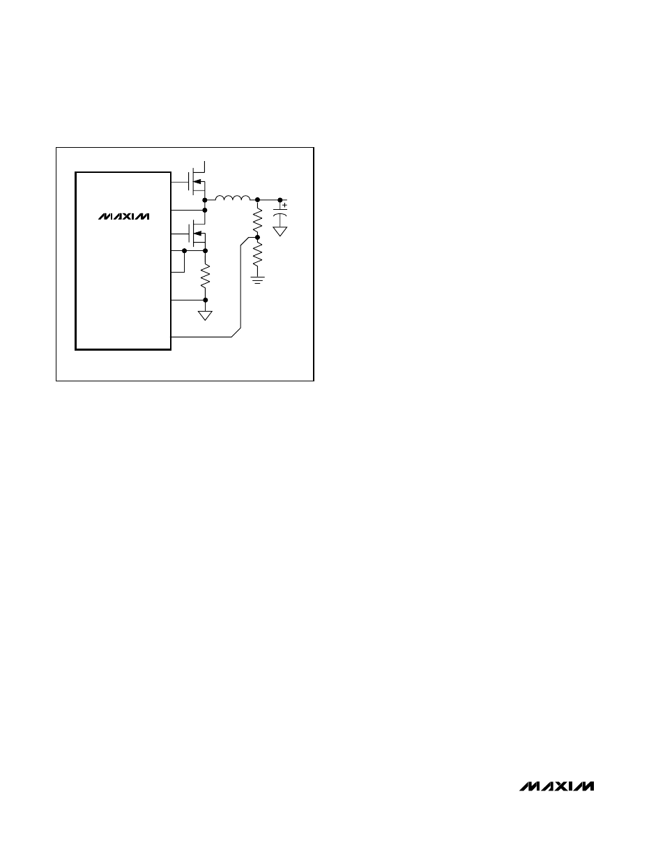
DH
LX
CS
VPS
DL
PGND
FB
V
OUT
Q2
Q1
R4
R5
L1
R
SENSE
V
OUT
= V
FB
(1 + R4/R5)
Figure 9. Adjusting V
OUT
with a Resistor-Divider