Pin description – Rainbow Electronics MAX1855 User Manual
Page 12
MAX1716/MAX1854/MAX1855
High-Speed, Adjustable, Synchronous Step-Down
Controllers with Integrated Voltage Positioning
12
______________________________________________________________________________________
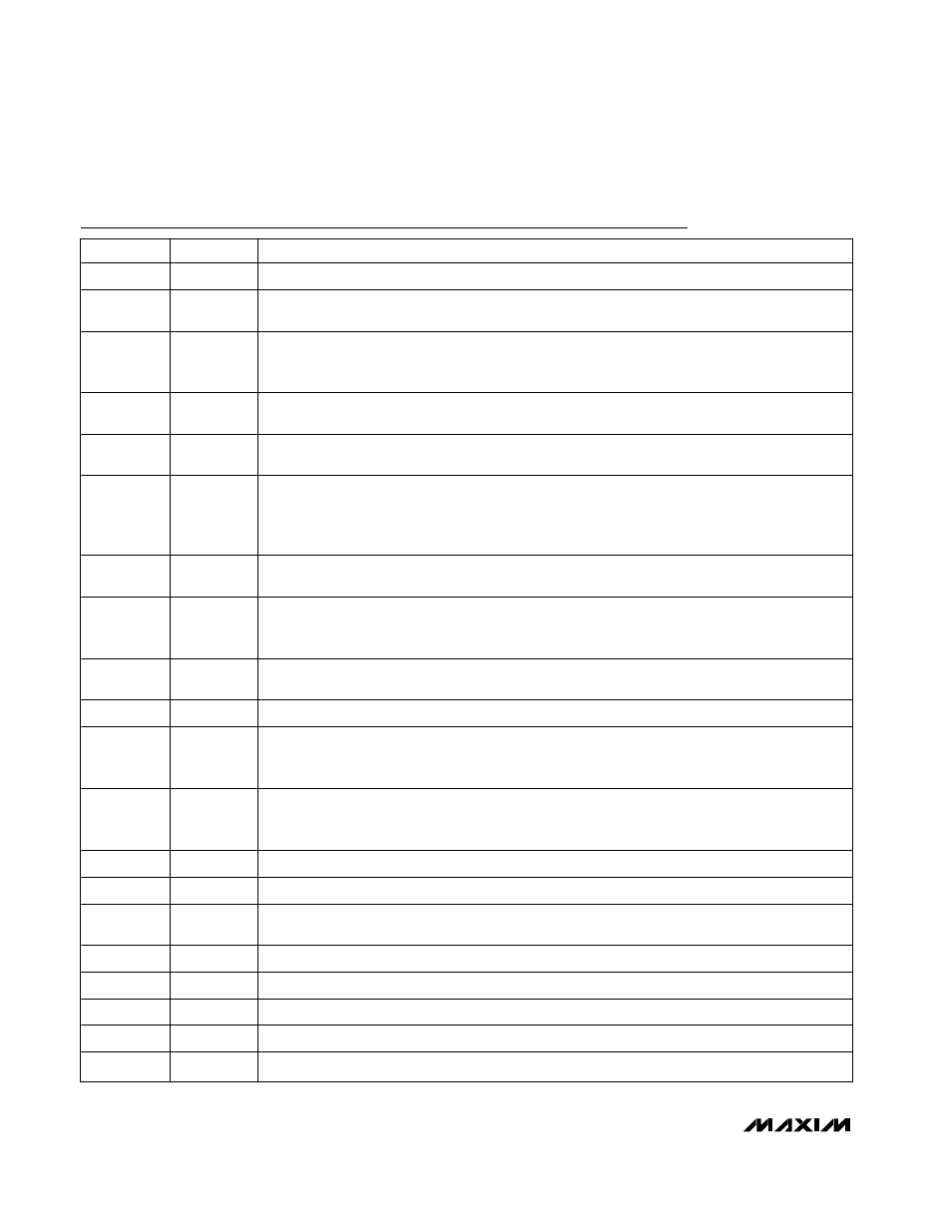
Pin Description
PIN
NAME
FUNCTION
1
DH
High-Side Gate Driver Output. DH swings from LX to BST.
2
V+
Battery Voltage Sense Connection. Connect V+ to input power source. V+ is used only for PWM
one-shot timing. DH on-time is inversely proportional to input voltage over a 2V to 28V range.
3
SHDN
Shutdown Control Input. Drive SHDN to GND to force the MAX1716/MAX1854/MAX1855 into
shutdown. Drive or connect to V
CC
for normal operation. A rising edge on SHDN clears the fault
latch.
4
FB
Feedback Input. Normally connected to V
OUT
. FB is connected to the bulk output filter capacitors
locally at the power supply. An external resistive divider can optionally set the output voltage.
5
CC
Voltage-Positioning Compensation Capacitor. Connect a 47pF to 1000pF (47pF typ) capacitor from
CC to GND to adjust the loop’s response time.
6
ILIM
Current-Limit Adjustment. The GND-CS current-limit threshold defaults to 120mV, if ILIM is tied to
V
CC
. In adjustable mode, the current-limit threshold voltage is 1/10th the voltage seen at ILIM over a
0.5V to 2.0V range. The logic threshold for switchover to the 120mV default value is approximately
V
CC
- 1V. Connect ILIM to REF for a fixed 200mV threshold.
7
V
CC
Analog Supply Input for PWM Core. Connect to the system supply voltage (+4.5V to +5.5V) with a
series 20
Ω resistor. Bypass to GND with a 0.22µF (min) ceramic capacitor.
8
TON
On-Time Selection-Control Input. This is a four-level input used to determine DH on-time. Connect to
GND, REF, or V
CC
, or leave TON unconnected to set the following switching frequencies: GND =
550kHz, REF = 400kHz, floating = 300kHz, and V
CC
= 200kHz.
9
REF
+2.0V Reference Voltage Output. Bypass to GND with 0.22
µF (min) capacitor. Can supply 50µA for
external loads.
10
GND
Analog Gound
11
VPS
Voltage-Positioning Sense Input. Connect to CS through a 1k
Ω resistor to maximize the load-
dependent output voltage drop, or adjust the voltage positioning level by connecting a resistive
divider from CS to PGND. Refer to Setting Voltage Positioning on how to select resistor values.
12
VGATE
Open-Drain Power-Good Output. VGATE is normally high when the output is in regulation. VGATE is
low in shutdown, undervoltage lockout, and during soft-start. Any fault condition forces VGATE low,
and it remains low until the fault is cleared.
13
DL
Low-Side Gate-Driver Output. DL swings from PGND to V
DD
.
14
PGND
Power Ground
15
V
DD
Supply Input for the DL Gate Drive. Connect to the system supply voltage, +4.5V to +5.5V. Bypass
to PGND with a 1
µF (min) ceramic capacitor.
16
D4
MSB DAC Code Input. 5
µA internal pullup to V
CC
(Table 5).
17
D3
DAC Code Input. 5
µA internal pullup to V
CC
(Table 5).
18
D2
DAC Code Input. 5
µA internal pullup to V
CC
(Table 5).
19
D1
DAC Code Input. 5
µA internal pullup to V
CC
(Table 5).
20
D0
LSB DAC Code Input. 5
µA internal pullup to V
CC
(Table 5).