Rainbow Electronics MAX1499 User Manual
Page 6

MAX1497/MAX1499
3.5- and 4.5-Digit, Single-Chip ADCs with LED
Drivers and µC Interface
6
_______________________________________________________________________________________
TIMING CHARACTERISTICS (Notes 11, 12, Figure 8)
(AV
DD
= DV
DD
= V
DD
= +2.7V to +5.25V, GND = 0, GLED = 0, V
LED
= +2.7V to +5.25V, V
REF+
- V
REF-
= 2.048V (external reference)
C
REF+
= C
REF-
= 0.1µF, C
VNEG
= 0.1µF. Internal clock mode, unless otherwise noted. All specifications are at T
A
= T
MIN
to T
MAX
.
Typical values are at T
A
= +25°C, unless otherwise noted.)
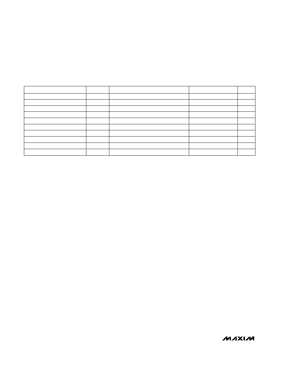
PARAMETER
SYMBOL
CONDITIONS
MIN
TYP
MAX
UNITS
SCLK Operating Frequency
f
SCLK
0
4.2
MHz
SCLK Pulse-Width High
t
CH
100
ns
SCLK Pulse-Width Low
t
CL
100
ns
DIN to SCLK Setup
t
DS
50
ns
DIN to SCLK Hold
t
DH
0
ns
CS Fall to SCLK Rise Setup
t
CSS
50
ns
SCLK Rise to CS Rise Hold
t
CSH
0
ns
SCLK Fall to DOUT Valid
t
DO
C
LOAD
= 50pF, Figures 13, 14
120
ns
CS Rise to DOUT Disable
t
TR
C
LOAD
= 50pF, Figures 13, 14
120
ns
CS Fall to DOUT Enable
t
DV
C
LOAD
= 50pF, Figures 13, 14
120
ns
Note 1: Integral nonlinearity is the deviation of the analog value at any code from its theoretical value after nulling the gain error and
offset error.
Note 2: Offset calibrated. See OFFSET_CAL1 and OFFSET_CAL2 (MAX1499 only) in the On-Chip Registers section.
Note 3: Offset nulled.
Note 4: Offset drift error is eliminated by recalibration at the new temperature.
Note 5: The input voltage range for the analog inputs is given with respect to the voltage on the negative input of the differential pair.
Note 6: V
AIN
+ or V
AIN
- = -2.2V to +2.2V. V
REF
+ or V
REF
- = -2.2V to +2.2V. All input structures are identical. Production tested on
AIN+ and REF+ only.
Note 7: Measured at DC by changing the power-supply voltage from 2.7V to 5.25V and measuring the effect on the conversion
error with external reference. PSRR at 50Hz and 60Hz exceeds 120dB with filter notches at 50Hz and 60Hz (Figure 2).
Note 8: CLK and SCLK are disabled.
Note 9: LED drivers are disabled.
Note 10: Power-supply currents are measured with all digital inputs at either GND, DV
DD
, or V
DD
and with the device in internal-clock mode.
Note 11: All input signals are specified with t
RISE
= t
FALL
= 5ns (10% to 90% of DV
DD
) and are timed from a voltage level of 50% of
DV
DD
, unless otherwise noted.
Note 12: See the serial-interface timing diagrams.
