Rainbow Electronics MAX1499 User Manual
Page 19
MAX1497/MAX1499
3.5- and 4.5-Digit, Single-Chip ADCs with LED
Drivers and µC Interface
______________________________________________________________________________________
19
Default values: 00h
This register contains the status of the conversion
results.
SIGN: Latched negative-polarity indicator. Latches
high when the result is negative. Clears by reading the
status register, unless the condition remains true.
OVER: Overrange bit. Latches high if an overrange
condition occurs (the ADC result is larger than the
value in the overrange register). Clears by reading the
status register, unless the condition remains true.
UNDER: Underrange bit. Latches high if an under-
range condition occurs (the ADC result is less than the
value in the underrange register). Clears by reading the
status register, unless the condition remains true.
LOW_BATT: Low-battery bit. Latches high if the volt-
age at the LOWBATT is lower than 2.048V (typ). Clears
by reading the status register, unless the condition
remains true. For the MAX1497, LOWBATT is not used
and the LOWBATT bit always returns to zero.
DRDY: Data ready bit. Latches high to indicate a com-
pleted conversion result with valid data. Read the ADC
result register to clear this bit.
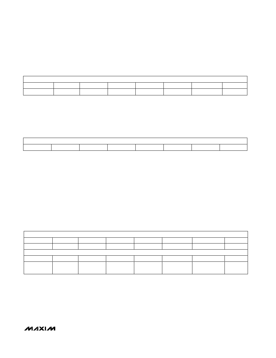
Control and Status Registers
Command Byte (Write Only)
Status Register (Read Only)
MSB
LSB
Bit 7
Bit 6
Bit 5
Bit 4
Bit 3
Bit 2
Bit 1
Bit 0
START(1)
R/W
RS4
RS3
RS2
RS1
RS0
X
MSB
LSB
SIGN
OVER
UNDER
LOW_BATT
DRDY
0
0
0
Control Register (Read/Write)
MSB
Bit 15
Bit 14
Bit 13
Bit 12
Bit 11
Bit 10
Bit 9
Bit 8
SPI/ADC
EXTCLK
INTREF
DPON
DPSET2
DPSET1
PD_DIG
PD_ANA
LSB
Bit 7
Bit 6
Bit 5
Bit 4
Bit 3
Bit 2
Bit 1
Bit 0
HOLD
PEAK
RANGE
CLR
SEG_SEL
OFFSET_CAL1
OFFSET_
CAL2
ENABLE
START: Start bit. The first 1 clocked into the MAX1497/
MAX1499 is the first bit of the command byte.
(R/W): Read/Write. Set this bit to 1 to read from the
specified register. Set this bit to zero to write to the
selected register. Note that certain registers are read
only. Write commands to a read-only register are
ignored.
(RS4–RS0): Register address bits. RS4 to RS0 specify
which register is accessed.
X: Don’t care.
Default values: 0001h
This register is the primary control register for the
MAX1497/MAX1499. It is a 16-bit read/write register. It
is used to indicate the desired clock and reference
source. It sets the LED display controls, range modes,
power-down modes, offset calibration, and the reset
register function (CLR).
ENABLE: (default = 1) LED driver enable bit. When set to
1, the MAX1497/MAX1499 enables the LED display dri-
vers. A 0 in this location disables the LED display drivers.
OFFSET_CAL2: (default = 0) Enhanced offset-calibra-
tion start bit (MAX1499, RANGE = 1). To achieve the
lowest possible offset in the ±200mV input range, per-
form an enhanced offset calibration by setting this bit to