Rainbow Electronics MAX1499 User Manual
Page 14
MAX1497/MAX1499
3.5- and 4.5-Digit, Single-Chip ADCs with LED
Drivers and µC Interface
14
______________________________________________________________________________________
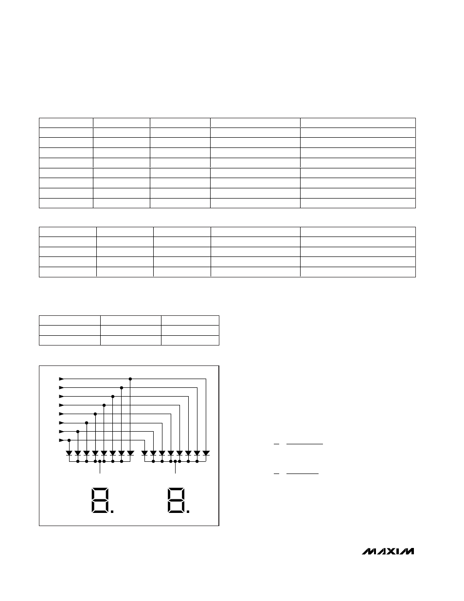
Figure 5 shows a typical common-cathode configura-
tion for two digits. In common-cathode configuration,
the cathodes of all LEDs in a digit are connected
together. Each segment driver of the MAX1497/
MAX1499 connects to its corresponding LEDs anodes.
For example, segment driver SEGA connects to all LED
segments designated as A. Similar configurations are
followed for other segment drivers.
The MAX1497/MAX1499 use a multiplexing scheme to
drive one digit at a time. The scan rate is fast enough to
make the digits appear to be lit. Figures 6 and 7 show
data timing diagrams for the MAX1497/MAX1499 where T
is the display scan period typically around 1/512Hz or
1.9531ms for the MAX1499 and 1/640Hz or 1.5625ms for
the MAX1497. T
ON
in Figures 6 and 7 denotes the amount
of time each digit is on and is calculated as follows:
The MAX1497/MAX1499 allow for full decimal-point
control and feature leading-zero suppression. Use the
DPON, DPSET1, and DPSET2 bits in the control register
to set the value of the decimal point (Tables 2 and 3).
The MAX1497/MAX1499 overrange and underrange
display is shown in Table 4.
T
T
ms
s MAX
T
T
ms
s MAX
ON
ON
=
=
=
=
=
=
5
1 95312
5
390 60
1499
4
1 5625
4
390 60
1497
.
.
(
)
.
.
(
)
µ
µ
A
A
A
DIGIT 1
DIGIT 2
SEGDP
SEGG
SEGF
SEGE
SEGD
SEGC
SEGB
SEGA
D
D
E
E
G
G
F
F
B
B
C
C
DP
DP
B
C
D
E
F
G
DP
A
B
C
D
E
F
G
DP
Figure 5. Two-Digit Common-Cathode Configuration
Table 2. Decimal-Point Control Table—MAX1499
DPON
DPSET1
DPSET2
DISPLAY OUTPUT
ZERO INPUT READING
0
0
0
18888
0
0
0
1
18888
0
0
1
0
18888
0
0
1
1
18888
0
1
0
0
1888.8
0.0
1
0
1
188.88
0.00
1
1
0
18.888
0.000
1
1
1
1.8888
0.0000
Table 3. Decimal-Point Control Table—MAX1497
DPON
DPSET1
DPSET2
DISPLAY OUTPUT
ZERO INPUT READING
X
0
0
188.8
0.0
X
0
1
18.88
0.00
X
1
0
1888
0
X
1
1
1.888
0.000
X = Don’t care.
Table 4. LED During Overrange and
Underrange Conditions
CONDITION
MAX1497
MAX1499
Overrange
1
---
1
----
Underrange
-
1
---
-
1
----