Applications information, Serial interface – Rainbow Electronics MAX1499 User Manual
Page 16
MAX1497/MAX1499
3.5- and 4.5-Digit, Single-Chip ADCs with LED
Drivers and µC Interface
16
______________________________________________________________________________________
Figure 15 shows the MAX1497/MAX1499 operating with
an external differential reference. In this mode, REF- is
connected to the top of the strain gauge and REF+ is
connected to the midpoint of the resistor-divider of
the supply.
Applications Information
Serial Interface
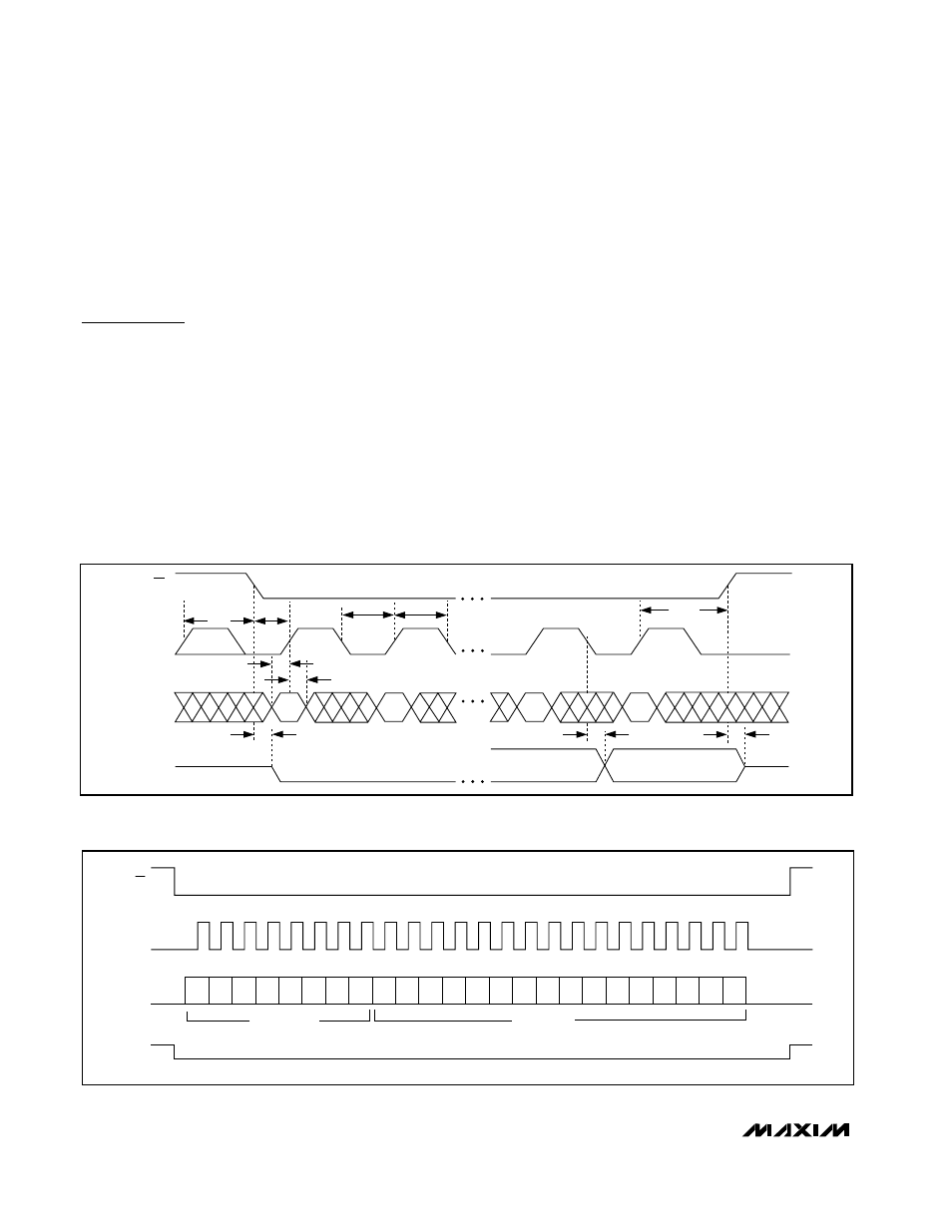
The SPI/QSPI/MICROWIRE serial interface consists of a
chip select (CS), a serial clock (SCLK), a data in (DIN),
a data out (DOUT), and an asynchronous EOC output.
EOC provides an asynchronous end-of-conversion sig-
nal with a period of 200ms (f
CLK
= 4.9152MHz). The
MAX1497 updates the data register when EOC goes
high. Data is valid in the ADC result registers when
EOC returns low. The serial interface provides access
to 12 on-chip registers, allowing control to all the power
modes and functional blocks. Table 5 lists the address
and read/write accessibility of all the registers.
A logic high on CS tri-states DOUT and causes the
MAX1497/MAX1499 to ignore any signals on SCLK and
DIN. To clock data in or out of the internal shift register,
drive CS low. SCLK synchronizes the data transfer. The
rising edge of SCLK clocks DIN into the shift register,
and the falling edge of SCLK clocks DOUT out of the
shift register. DIN and DOUT are transferred MSB first
(data is left justified). Figures 8–12 show the detailed
serial interface timing diagrams for the 8- and 16-bit
read/write operations.
All communication with the MAX1497/MAX1499 begins
with a command byte on DIN, where the first logic one
on DIN is recognized as the START bit (MSB) for the
command byte. The following seven clock cycles load
the command into a shift register. These 7 bits specify
which of the registers are accessed next, and whether
a read or write operation takes place. Transitions on the
serial clock after the command byte transfer, cause a
write or read from the device until the correct number of
CS
SCLK
DIN
DOUT
t
CSH
t
CL
t
DS
t
DH
t
DV
t
CH
t
DO
t
TR
t
CSH
t
CSS
Figure 8. Detailed Timing Diagram
SCLK
CS
DIN
DOUT
1
0
RS4 RS3
RS2 RS1
D7
D6
D5
D4
D3
D2
D1
D0
D8
D9
RS0
x
D15 D14 D13 D12 D11 D10
CONTROL BYTE
DATA BYTE
Figure 9. Serial-Interface, 16-Bit, Write Timing Diagram