Table 6. segment current selection – Rainbow Electronics MAX1499 User Manual
Page 27
The transfer function for the MAX1499 with AIN+ - AIN-
< 0, RANGE = 0 is:
The transfer function for the MAX1497 with AIN+ - AIN-
≥ 0, RANGE = 0 is:
The transfer function for the MAX1497 with AIN+ - AIN-
< 0, RANGE = 0 is:
The transfer function for the MAX1499 with AIN+ - AIN-
≥ 0, RANGE = 1 is:
The transfer function for the MAX1499 with AIN+ - AIN-
< 0, RANGE = 1 is:
The transfer function for the MAX1497 with AIN+ - AIN-
≥ 0, RANGE = 1 is:
The transfer function for the MAX1497 with AIN+ - AIN-
< 0, RANGE = 1 is:
Supplies, Layout, and Bypassing
Power up AVDD and DVDD (MAX1499) and VDD
(MAX1497) before applying an analog input and exter-
nal reference voltage to the device. If this is not possi-
ble, limit the current into these inputs to 50mA. When
the analog and digital supplies come from the same
source, isolate the digital supply from the analog sup-
ply with a low-value resistor (10Ω) or ferrite bead. For
best performance, ground the MAX1497/MAX1499 to
the analog ground plane of the circuit board.
Avoid running digital lines under the device, because
they may couple noise onto the die. Run the analog
ground plane under the MAX1497/MAX1499 to mini-
mize coupling of digital noise. Make the power-supply
lines to the MAX1497/MAX1499 as wide as possible to
provide low-impedance paths and reduce the effects of
glitches on the power-supply line.
Shield fast-switching signals, such as clocks, with digital
ground to avoid radiating noise to other sections of the
board. Avoid running clock signals near the analog
inputs. Avoid crossover of digital and analog signals.
Running traces that are on opposite sides of the board at
right angles to each other reduces feedthrough effects.
A microstrip technique is best, but is not always possible
with double-sided boards. With this technique, the com-
ponent side of the board is dedicated to ground planes
while signals are placed on the solder side.
Good decoupling is important when using high-resolution
ADCs. Decouple the supplies with 0.1µF ceramic capaci-
tors to GND. Place these components as close to the
device as possible to achieve the best decoupling.
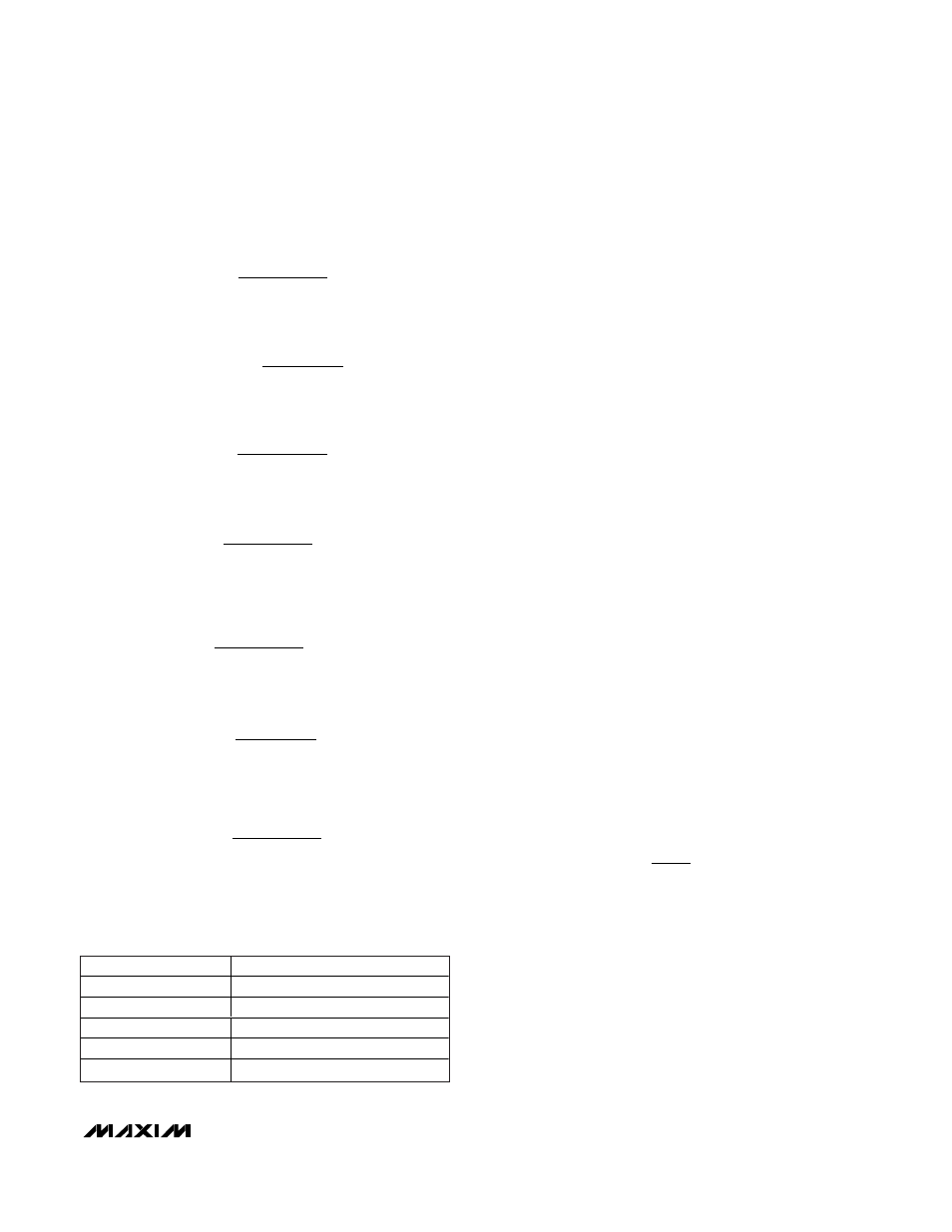
Segment-Current Selection
A resistor from ISET to ground sets the current for each
LED segment. See Table 6 for more detail. Use the fol-
lowing formula to set the segment current:
R
ISET
values below 25kΩ increase the I
SEG
. However,
the internal current-limit circuit limits the I
SEG
to less than
30mA. At higher I
SEG
values, the proper operation of the
device is not guaranteed. In addition, the power dissipat-
ed may exceed the package power dissipation limit.
I
V
R
SEG
ISET
=
×
1 25
400
.
COUNTS
V
V
V
V
AIN
AIN
REF
REF
.
=
Ч
Ч
+
+
+
−
−
−
−
1 024
2000
10
1
COUNTS
V
V
V
V
AIN
AIN
REF
REF
.
=
Ч
Ч
+
−
+
−
−
−
1 024
2000
10
COUNTS
V
V
V
V
AIN
AIN
REF
REF
.
,
=
Ч
Ч
+
+
+
−
−
−
−
1 024
20 000
10
1
COUNTS
V
V
V
V
AIN
AIN
REF
REF
.
,
=
Ч
Ч
+
+
−
−
−
−
1 024
20 000
10
COUNTS
V
V
V
V
AIN
AIN
REF
REF
.
=
×
+
+
+
−
−
−
−
1 024
2000
1
COUNTS
V
V
V
V
AIN
AIN
REF
REF
.
=
×
+
−
+
−
−
−
1 024
2000
COUNTS
V
V
V
V
AIN
AIN
REF
REF
.
,
=
×
+
+
+
−
−
−
−
1 024
20 000
1
MAX1497/MAX1499
3.5- and 4.5-Digit, Single-Chip ADCs with LED
Drivers and µC Interface
______________________________________________________________________________________
27
R
ISET
(k
Ω
)
I
SEG
(mA)
25
20
50
10
100
5
500
1
>2500
LED driver disabled
Table 6. Segment Current Selection