Power-on reset, Offset calibration, Enhanced offset calibration – Rainbow Electronics MAX1499 User Manual
Page 25: Power-down modes, Peak, Hold, Low battery, Strain-gauge measurement
MAX1497/MAX1499
3.5- and 4.5-Digit, Single-Chip ADCs with LED
Drivers and µC Interface
______________________________________________________________________________________
25
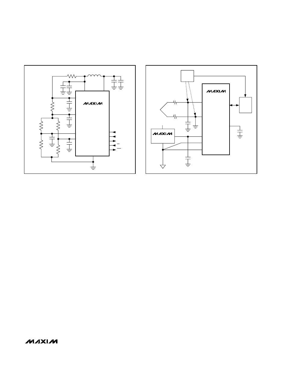
Figure 16. Thermocouple Application with the MAX1497/MAX1499
Figure 15. Strain-Gauge Application with the MAX1497/MAX1499
MAX1497
MAX1499
AV
DD
DV
DD
DOUT
DIN
SCLK
4.7µF
0.1µF
0.1µF
0.1µF
0.1µF
0.1µF
ANALOG SUPPLY
FERRITE
BEAD
R
REF
R
R
ACTIVE
GAUGE
DUMMY
GAUGE
REF+
REF-
AIN+
AIN-
GND
EOC
CS
4.7µF
0.1µF
MAX1497
MAX1499
MAX6062
+5V
+2.048V
TEMP
SENSOR
THERMOCOUPLE
JUNCTION
0.1µF
0.47µF
SPI
µC
AIN+
AIN-
REF+
REF-
GND
Power-On Reset
At power-on, the serial interface, logic LED drivers, dig-
ital filter, and modulator circuits reset. The registers
return to their default values. Allow time for the refer-
ence to settle before starting calibration.
Offset Calibration
The MAX1497/MAX1499 offer on-chip offset calibration.
The device offset calibrates during every conversion
when the OFFSET_CAL1 bit is zero in the control regis-
ter. Enhanced offset calibration is only needed in the
MAX1499 when the RANGE bit = 1. It is performed on
demand by setting the OFFSET_CAL2 bit to 1.
Enhanced Offset Calibration
Enhanced offset calibration is a more accurate calibra-
tion method that is needed in the case of the ±200mV
range and 4.5-digit resolution. The MAX1499 performs
the enhanced calibration on demand by setting the
OFFSET_CAL2 bit to 1.
Power-Down Modes
The MAX1497/MAX1499 feature independent power-
down control of the analog and digital LED drivers cir-
cuitry. Writing a 1 to the PD_DIG and PD_ANA bits in
the control word, powers down the analog and digital
circuitry, reducing the supply current to 268µA (typ).
PD_DIG powers down the digital filter, while PD_ANA
powers down the analog modulator and ADC input
buffers. Writing a zero to the ENABLE bit in the control
word, powers down the LED drivers.
Peak
The MAX1497/MAX1499 feature peak detection circuit-
ry. When activated (PEAK bit = 1), the devices display
only the highest voltage measured to the LED.
Hold
The MAX1497/MAX1499 feature data-hold circuitry.
When activated (HOLD bit = 1), the device displays the
current reading on the LED.
Low Battery
The MAX1499 features a low-battery detection input.
When the voltage at LOWBATT drops below 2.048V
(typ), the LOWBATT bit of the status register goes high.
Strain-Gauge Measurement
Connect the differential inputs of the MAX1497/MAX1499
to the bridge network of the strain gauge. In Figure 15,
the analog supply voltage powers the bridge network
and the MAX1497/MAX1499 along with the reference
voltage. The MAX1497/MAX1499 handle an analog input
voltage range of ±200mV and ±2V full scale. The ana-
log/reference inputs of the parts allow the analog input
range to have an absolute value of anywhere between
-2.2V and +2.2V.