Pin description – Rainbow Electronics MAX1499 User Manual
Page 10
MAX1497/MAX1499
3.5- and 4.5-Digit, Single-Chip ADCs with LED
Drivers and µC Interface
10
______________________________________________________________________________________
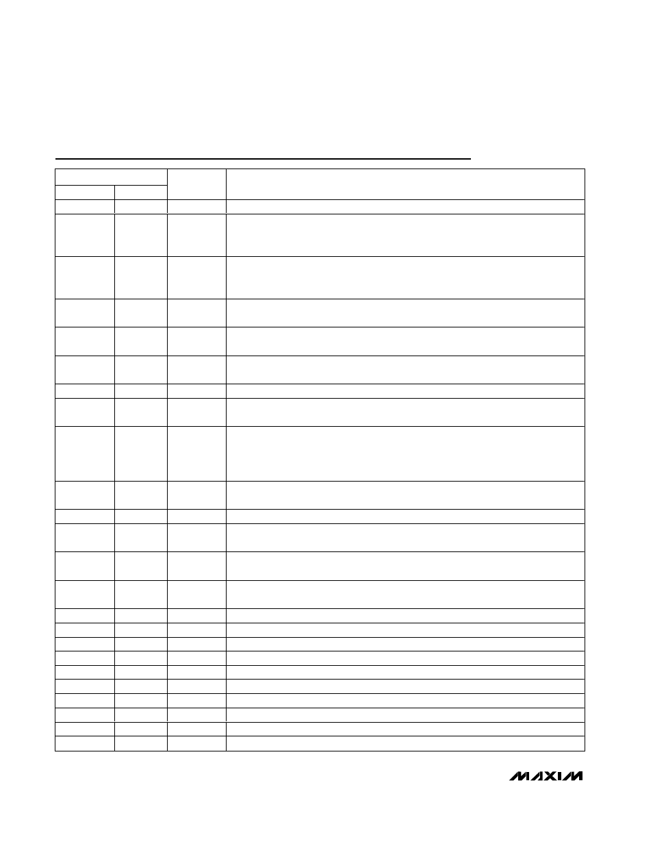
Pin Description
PIN
MAX1497
MAX1499
NAME
FUNCTION
1
31
VNEG
-2.5V Charge-Pump Voltage-Output. Connect a 0.1µF capacitor to GND.
2
32
REF-
Negative Reference Voltage Input. For internal reference operation, connect REF- to
GND. For external reference operation, bypass REF- to GND with a 0.1µF capacitor and
set V
REF-
from -2.2V to +2.2V, provided V
REF+
> V
REF-
.
3
1
REF+
Positive Reference Voltage Input. For internal reference operation, connect a 4.7µF
capacitor from REF+ to GND. For external reference operation, bypass REF+ to GND
with a 0.1µF capacitor and set V
REF+
from -2.2V to +2.2V, provided V
REF+
> V
REF-
.
4
2
AIN+
Positive Analog Input. Positive side of fully differential analog input. Bypass AIN+ to GND
with a 0.1µF or greater capacitor.
5
3
AIN-
Negative Analog Input. Negative side of fully differential analog input. Bypass AIN- to
GND with a 0.1µF or greater capacitor.
6
4
I
SET
Segment Current Controller. Connect to ground through a resistor to set the segment
current. See Table 6 for segment current selection.
7
5
GND
Ground
8
—
V
DD
Analog and Digital Circuit Supply Voltage. Connect V
DD
to a +2.7V to +5.25V power
supply. Bypass V
DD
to GND with a 0.1µF and a 4.7µF capacitor.
9
8
CLK
External Clock Input. When the EXTCLK register bit is set to one, CLK is the master clock
input (frequency = 4.9152MHz) for the modulator and the filter. When the EXTCLK
register bit is reset to zero, the internal clock is used. Connect CLK to GND or DV
DD
(MAX1499) or V
DD
(MAX1497) when the internal oscillator is used.
10
9
EOC
Active-Low End-of-Conversion Logic Output. A logic low at EOC indicates that a new
ADC result is available in the ADC result register.
11
10
CS
Active-Low Chip Select Input. Forcing CS low activates the serial interface.
12
11
DIN
Serial Data Input. Data present at DIN is shifted into the internal registers in response to
a rising edge at SCLK when CS is low.
13
12
SCLK
Serial Clock Input. Apply an external clock to SCLK to facilitate communication through
the serial bus. SCLK may idle high or low.
14
13
DOUT
Serial Data Output. DOUT presets serial data in response to register queries. Data shifts
out on the falling edge of SCLK. DOUT goes high impedance when CS is high.
15
14
DIG0
Digit 0 Driver
16
15
DIG1
Digit 1 Driver
17
16
GLED
Ground for LED-Display Segment Driver
18
17
DIG2
Digit 2 Driver
19
18
DIG3
Digit 3 Driver
20
20
SEGA
Segment A Driver
21
21
SEGB
Segment B Driver
22
22
SEGC
Segment C Driver
23
23
SEGD
Segment D Driver
24
24
SEGE
Segment E Driver